MA180023 Microchip Technology, MA180023 Datasheet - Page 94
MA180023
Manufacturer Part Number
MA180023
Description
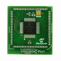
MODULE PLUG-IN PIC18F46J11 PIM
Manufacturer
Microchip Technology
Series
PIC®r
Datasheet
1.MA180023.pdf
(528 pages)
Specifications of MA180023
Accessory Type
Plug-In Module (PIM) - PIC18F46J11
Tool / Board Applications
General Purpose MCU, MPU, DSP, DSC
Mcu Supported Families
PIC18
Supported Devices
Stand-alone Or W/ HPC(DM183022) Or PIC18(DM183032)
Silicon Manufacturer
Microchip
Core Architecture
PIC
Core Sub-architecture
PIC18
Silicon Core Number
PIC18F
Silicon Family Name
PIC18FxxJxx
Lead Free Status / RoHS Status
Lead free / RoHS Compliant
For Use With/related Products
HPC Explorer Board (DM183022) or PIC18 Explorer Board (DM183032)
For Use With
DM183032 - BOARD EXPLORER PICDEM PIC18DM183022 - BOARD DEMO PIC18FXX22 64/80TQFP
Lead Free Status / RoHS Status
Lead free / RoHS Compliant
Available stocks
Company
Part Number
Manufacturer
Quantity
Price
Company:

Part Number:
MA180023
Manufacturer:
Microchip Technology
Quantity:
135


PIC18F46J11 FAMILY
FIGURE 5-9:
DS39932C-page 94
EXAMPLE INSTRUCTION: ADDWF, f, d, a (Opcode: 0010 01da ffff ffff)
When a = 0 and f ≥ 60h:
The instruction executes in
Direct Forced mode. ‘f’ is
interpreted as a location in the
Access RAM between 060h
and FFFh. This is the same as
locations
(Bank 15) of data memory.
Locations below 060h are not
available in this addressing
mode.
When a = 0 and f ≤ 5Fh:
The instruction executes in
Indexed Literal Offset mode. ‘f’
is interpreted as an offset to the
address value in FSR2. The
two are added together to
obtain the address of the target
register for the instruction. The
address can be anywhere in
the data memory space.
Note that in this mode, the
correct syntax is:
ADDWF [k], d
where ‘k’ is same as ‘f’.
When a = 1 (all values of f):
The instruction executes in
Direct mode (also known as
Direct Long mode). ‘f’ is
interpreted as a location in
one of the 16 banks of the data
memory space. The bank is
designated by the Bank Select
Register (BSR). The address
can be in any implemented
bank in the data memory
space.
F60h
COMPARING ADDRESSING OPTIONS FOR BIT-ORIENTED AND BYTE-ORIENTED
INSTRUCTIONS (EXTENDED INSTRUCTION SET ENABLED)
to
FFFh
FFFh
FFFh
FFFh
F00h
F60h
F00h
F60h
F00h
F60h
000h
060h
100h
000h
060h
100h
000h
060h
100h
Data Memory
Data Memory
Data Memory
Bank 15
Bank 15
Bank 15
Bank 14
Bank 14
Bank 14
Bank 0
through
Bank 0
through
Bank 0
through
Bank 1
Bank 1
Bank 1
SFRs
SFRs
SFRs
001001da
00000000
001001da
BSR
Access RAM
© 2009 Microchip Technology Inc.
FSR2H
ffffffff
ffffffff
FSR2L
FFh
00h
60h
Valid range
for ‘f’
Related parts for MA180023
Image
Part Number
Description
Manufacturer
Datasheet
Request
R

Part Number:
Description:
Manufacturer:
Microchip Technology Inc.
Datasheet:
Part Number:
Description:
Manufacturer:
Microchip Technology Inc.
Datasheet:
Part Number:
Description:
Manufacturer:
Microchip Technology Inc.
Datasheet:
Part Number:
Description:
Manufacturer:
Microchip Technology Inc.
Datasheet:
Part Number:
Description:
Manufacturer:
Microchip Technology Inc.
Datasheet:
Part Number:
Description:
Manufacturer:
Microchip Technology Inc.
Datasheet:
Part Number:
Description:
Manufacturer:
Microchip Technology Inc.
Datasheet:
Part Number:
Description:
Manufacturer:
Microchip Technology Inc.
Datasheet: