MA180023 Microchip Technology, MA180023 Datasheet - Page 306
MA180023
Manufacturer Part Number
MA180023
Description
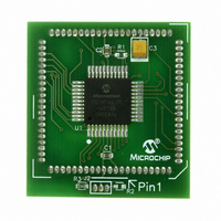
MODULE PLUG-IN PIC18F46J11 PIM
Manufacturer
Microchip Technology
Series
PIC®r
Datasheet
1.MA180023.pdf
(528 pages)
Specifications of MA180023
Accessory Type
Plug-In Module (PIM) - PIC18F46J11
Tool / Board Applications
General Purpose MCU, MPU, DSP, DSC
Mcu Supported Families
PIC18
Supported Devices
Stand-alone Or W/ HPC(DM183022) Or PIC18(DM183032)
Silicon Manufacturer
Microchip
Core Architecture
PIC
Core Sub-architecture
PIC18
Silicon Core Number
PIC18F
Silicon Family Name
PIC18FxxJxx
Lead Free Status / RoHS Status
Lead free / RoHS Compliant
For Use With/related Products
HPC Explorer Board (DM183022) or PIC18 Explorer Board (DM183032)
For Use With
DM183032 - BOARD EXPLORER PICDEM PIC18DM183022 - BOARD DEMO PIC18FXX22 64/80TQFP
Lead Free Status / RoHS Status
Lead free / RoHS Compliant
Available stocks
Company
Part Number
Manufacturer
Quantity
Price
Company:

Part Number:
MA180023
Manufacturer:
Microchip Technology
Quantity:
135


PIC18F46J11 FAMILY
A typical transmit sequence would go as follows:
1.
2.
3.
4.
5.
6.
7.
8.
9.
10. The MSSP module generates an interrupt at the
11. The user generates a Stop condition by setting
12. Interrupt is generated once the Stop condition is
DS39932C-page 306
The user generates a Start condition by setting
the Start Enable bit, SEN (SSPxCON2<0>).
SSPxIF is set. The MSSP module will wait for
the required start time before any other
operation takes place.
The user loads the SSPxBUF with the slave
address to transmit.
Address is shifted out of the SDAx pin until all
8 bits are transmitted.
The MSSP module shifts in the ACK bit from the
slave device and writes its value into the
SSPxCON2 register (SSPxCON2<6>).
The MSSP module generates an interrupt at the
end of the ninth clock cycle by setting the
SSPxIF bit.
The user loads the SSPxBUF with 8 bits of data.
Data is shifted out the SDAx pin until all 8 bits
are transmitted.
The MSSP module shifts in the ACK bit from the
slave device and writes its value into the
SSPxCON2 register (SSPxCON2<6>).
end of the ninth clock cycle by setting the
SSPxIF bit.
the Stop Enable bit, PEN (SSPxCON2<2>).
complete.
18.5.7
In I
the lower seven bits of the SSPxADD register
(Figure 18-19). When a write occurs to SSPxBUF, the
Baud Rate Generator will automatically begin counting.
The BRG counts down to 0 and stops until another
reload has taken place. The BRG count is decre-
mented twice per instruction cycle (T
Q4 clocks. In I
automatically.
Once the given operation is complete (i.e., transmis-
sion of the last data bit is followed by ACK), the internal
clock will automatically stop counting and the SCLx pin
will remain in its last state.
Table 18-3 demonstrates clock rates based on
instruction cycles and the BRG value loaded into
SSPxADD.
2
C Master mode, the BRG reload value is placed in
BAUD RATE
2
C Master mode, the BRG is reloaded
© 2009 Microchip Technology Inc.
CY
) on the Q2 and
Related parts for MA180023
Image
Part Number
Description
Manufacturer
Datasheet
Request
R

Part Number:
Description:
Manufacturer:
Microchip Technology Inc.
Datasheet:
Part Number:
Description:
Manufacturer:
Microchip Technology Inc.
Datasheet:
Part Number:
Description:
Manufacturer:
Microchip Technology Inc.
Datasheet:
Part Number:
Description:
Manufacturer:
Microchip Technology Inc.
Datasheet:
Part Number:
Description:
Manufacturer:
Microchip Technology Inc.
Datasheet:
Part Number:
Description:
Manufacturer:
Microchip Technology Inc.
Datasheet:
Part Number:
Description:
Manufacturer:
Microchip Technology Inc.
Datasheet:
Part Number:
Description:
Manufacturer:
Microchip Technology Inc.
Datasheet: