MA180023 Microchip Technology, MA180023 Datasheet - Page 522
MA180023
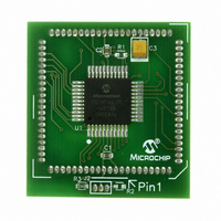
Manufacturer Part Number
MA180023
Description
MODULE PLUG-IN PIC18F46J11 PIM
Manufacturer
Microchip Technology
Series
PIC®r
Datasheet
1.MA180023.pdf
(528 pages)
Specifications of MA180023
Accessory Type
Plug-In Module (PIM) - PIC18F46J11
Tool / Board Applications
General Purpose MCU, MPU, DSP, DSC
Mcu Supported Families
PIC18
Supported Devices
Stand-alone Or W/ HPC(DM183022) Or PIC18(DM183032)
Silicon Manufacturer
Microchip
Core Architecture
PIC
Core Sub-architecture
PIC18
Silicon Core Number
PIC18F
Silicon Family Name
PIC18FxxJxx
Lead Free Status / RoHS Status
Lead free / RoHS Compliant
For Use With/related Products
HPC Explorer Board (DM183022) or PIC18 Explorer Board (DM183032)
For Use With
DM183032 - BOARD EXPLORER PICDEM PIC18DM183022 - BOARD DEMO PIC18FXX22 64/80TQFP
Lead Free Status / RoHS Status
Lead free / RoHS Compliant
Available stocks
Company
Part Number
Manufacturer
Quantity
Price
Company:

Part Number:
MA180023
Manufacturer:
Microchip Technology
Quantity:
135


PIC18F46J11 FAMILY
DS39932C-page 522
Asynchronous Transmission (Back-to-Back) ........... 332
Automatic Baud Rate Calculation ............................ 330
Auto-Wake-up Bit (WUE) During Normal Operation 335
Auto-Wake-up Bit (WUE) During Sleep ................... 335
Baud Rate Generator with Clock Arbitration ............ 308
BRG Overflow Sequence ......................................... 330
BRG Reset Due to SDAx Arbitration During Start Condi-
Bus Collision During a Repeated Start Condition (Case
Bus Collision During a Repeated Start Condition (Case
Bus Collision During a Start Condition (SCLx = 0) ... 316
Bus Collision During a Stop Condition (Case 1) ...... 318
Bus Collision During a Stop Condition (Case 2) ...... 318
Bus Collision During Start Condition (SDAx Only) ... 315
Bus Collision for Transmit and Acknowledge ........... 314
CLKO and I/O .......................................................... 482
Clock Synchronization ............................................. 301
Clock/Instruction Cycle .............................................. 76
Enhanced Capture/Compare/PWM ......................... 485
EUSARTx Synchronous Receive (Master/Slave) .... 496
EUSARTx Synchronous Transmission (Master/Slave) ..
Example SPI Master Mode (CKE = 0) ..................... 488
Example SPI Master Mode (CKE = 1) ..................... 489
Example SPI Slave Mode (CKE = 0) ....................... 490
Example SPI Slave Mode (CKE = 1) ....................... 491
External Clock .......................................................... 480
Fail-Safe Clock Monitor ............................................ 404
First Start Bit ............................................................ 308
Full-Bridge PWM Output .......................................... 254
Half-Bridge PWM Output ................................. 252, 259
High/Low-Voltage Detect Characteristics ................ 478
High-Voltage Detect (VDIRMAG = 1) ....................... 371
I
I
I
I
I
I
I
I
I
I
I
I
I
I
I
Low-Voltage Detect (VDIRMAG = 0) ....................... 370
MSSPx I
MSSPx I
Parallel Master Port Read ........................................ 486
Parallel Master Port Write ........................................ 487
Parallel Slave Port Read .................................. 175, 177
Parallel Slave Port Write .................................. 175, 178
PWM Auto-Shutdown with Auto-Restart Enabled .... 258
PWM Auto-Shutdown with Firmware Restart ........... 258
PWM Direction Change ........................................... 255
PWM Direction Change at Near 100% Duty Cycle .. 256
PWM Output ............................................................ 246
2
2
2
2
2
2
2
2
2
2
2
2
2
2
2
2C Bus Data .......................................................... 492
C Acknowledge Sequence .................................... 313
C Bus Start/Stop Bits ............................................. 492
C Master Mode (7 or 10-Bit Transmission) ........... 311
C Master Mode (7-Bit Reception) .......................... 312
C Slave Mode (10-Bit Reception, SEN = 0, ADMSK =
C Slave Mode (10-Bit Reception, SEN = 0) .......... 298
C Slave Mode (10-Bit Reception, SEN = 1) .......... 303
C Slave Mode (10-Bit Transmission) ..................... 299
C Slave Mode (7-Bit Reception, SEN = 0, ADMSK =
C Slave Mode (7-Bit Reception, SEN = 0) ............ 294
C Slave Mode (7-Bit Reception, SEN = 1) ............ 302
C Slave Mode (7-Bit Transmission) ....................... 296
C Slave Mode General Call Address Sequence (7 or
C Stop Condition Receive or Transmit Mode ........ 313
tion ................................................................... 316
1) ...................................................................... 317
2) ...................................................................... 317
496
01001) .............................................................. 297
01011) .............................................................. 295
10-Bit Addressing Mode) ................................. 304
2
2
C Bus Data ............................................... 494
C Bus Start/Stop Bits ................................ 494
PWM Output (Active-High) ...................................... 250
PWM Output (Active-Low) ....................................... 251
Read and Write, 8-Bit Data, Demultiplexed Address 182
Read, 16-Bit Data, Demultiplexed Address ............. 185
Read, 16-Bit Multiplexed Data, Fully Multiplexed 16-Bit
Read, 16-Bit Multiplexed Data, Partially Multiplexed Ad-
Read, 8-Bit Data, Fully Multiplexed 16-Bit Address . 184
Read, 8-Bit Data, Partially Multiplexed Address ...... 182
Read, 8-Bit Data, Partially Multiplexed Address, Enable
Read, 8-Bit Data, Wait States Enabled, Partially Multi-
Repeated Start Condition ........................................ 309
Reset, Watchdog Timer (WDT), Oscillator Start-up Timer
Send Break Character Sequence ............................ 336
Slave Synchronization ............................................. 272
Slow Rise Time (MCLR Tied to V
SPI Mode (Master Mode) ......................................... 271
SPI Mode (Slave Mode, CKE = 0) ........................... 273
SPI Mode (Slave Mode, CKE = 1) ........................... 273
Steering Event at Beginning of Instruction (STRSYNC =
Steering Event at End of Instruction (STRSYNC = 0) ...
Synchronous Reception (Master Mode, SREN) ...... 339
Synchronous Transmission ..................................... 337
Synchronous Transmission (Through TXEN) .......... 338
Time-out Sequence on Power-up (MCLR Not Tied to
Time-out Sequence on Power-up (MCLR Not Tied to
Time-out Sequence on Power-up (MCLR Tied to V
Timer Pulse Generation ........................................... 238
Timer0 and Timer1 External Clock .......................... 484
Timer1 Gate Count Enable Mode ............................ 203
Timer1 Gate Single Pulse Mode .............................. 205
Timer1 Gate Single Pulse/Toggle Combined Mode 206
Timer1 Gate Toggle Mode ....................................... 204
Timer3 Gate Count Enable Mode) ........................... 213
Timer3 Gate Single Pulse Mode .............................. 215
Timer3 Gate Single Pulse/Toggle Combined Mode 216
Timer3 Gate Toggle Mode ....................................... 214
Transition for Entry to Idle Mode ................................ 47
Transition for Entry to SEC_RUN Mode .................... 43
Transition for Entry to Sleep Mode ............................ 45
Transition for Two-Speed Start-up (INTRC to HSPLL) ..
Transition for Wake From Idle to Run Mode .............. 47
Transition for Wake From Sleep (HSPLL) ................. 45
Transition From RC_RUN Mode to PRI_RUN Mode . 44
Transition From SEC_RUN Mode to PRI_RUN Mode
Transition to RC_RUN Mode ..................................... 44
Write, 16-Bit Data, Demultiplexed Address ............. 185
Write, 16-Bit Multiplexed Data, Fully Multiplexed 16-Bit
Write, 16-Bit Multiplexed Data, Partially Multiplexed Ad-
Write, 8-Bit Data, Fully Multiplexed 16-Bit Address . 184
Write, 8-Bit Data, Partially Multiplexed Address ...... 183
Address ........................................................... 186
dress ................................................................ 185
Strobe .............................................................. 183
plexed Address ................................................ 182
(OST) and Power-up Timer (PWRT) ............... 483
1) ..................................................................... 262
262
V
V
V
403
(HSPLL) ............................................................. 43
Address ........................................................... 186
dress ................................................................ 186
............................................................................ 61
DD
DD
DD
), Case 1 ..................................................... 61
), Case 2 ..................................................... 61
Rise < T
PWRT
© 2009 Microchip Technology Inc.
) ............................................ 60
DD
, V
DD
Rise > T
PWRT
DD
)
,
Related parts for MA180023
Image
Part Number
Description
Manufacturer
Datasheet
Request
R

Part Number:
Description:
Manufacturer:
Microchip Technology Inc.
Datasheet:
Part Number:
Description:
Manufacturer:
Microchip Technology Inc.
Datasheet:
Part Number:
Description:
Manufacturer:
Microchip Technology Inc.
Datasheet:
Part Number:
Description:
Manufacturer:
Microchip Technology Inc.
Datasheet:
Part Number:
Description:
Manufacturer:
Microchip Technology Inc.
Datasheet:
Part Number:
Description:
Manufacturer:
Microchip Technology Inc.
Datasheet:
Part Number:
Description:
Manufacturer:
Microchip Technology Inc.
Datasheet:
Part Number:
Description:
Manufacturer:
Microchip Technology Inc.
Datasheet: