MA180023 Microchip Technology, MA180023 Datasheet - Page 266
MA180023
Manufacturer Part Number
MA180023
Description
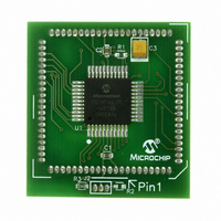
MODULE PLUG-IN PIC18F46J11 PIM
Manufacturer
Microchip Technology
Series
PIC®r
Datasheet
1.MA180023.pdf
(528 pages)
Specifications of MA180023
Accessory Type
Plug-In Module (PIM) - PIC18F46J11
Tool / Board Applications
General Purpose MCU, MPU, DSP, DSC
Mcu Supported Families
PIC18
Supported Devices
Stand-alone Or W/ HPC(DM183022) Or PIC18(DM183032)
Silicon Manufacturer
Microchip
Core Architecture
PIC
Core Sub-architecture
PIC18
Silicon Core Number
PIC18F
Silicon Family Name
PIC18FxxJxx
Lead Free Status / RoHS Status
Lead free / RoHS Compliant
For Use With/related Products
HPC Explorer Board (DM183022) or PIC18 Explorer Board (DM183032)
For Use With
DM183032 - BOARD EXPLORER PICDEM PIC18DM183022 - BOARD DEMO PIC18FXX22 64/80TQFP
Lead Free Status / RoHS Status
Lead free / RoHS Compliant
Available stocks
Company
Part Number
Manufacturer
Quantity
Price
Company:

Part Number:
MA180023
Manufacturer:
Microchip Technology
Quantity:
135


registers. These include a status register (SSPxSTAT)
PIC18F46J11 FAMILY
18.2
Each MSSP module has three associated control
and two control registers (SSPxCON1 and SSPxCON2).
The use of these registers and their individual Configura-
tion bits differ significantly depending on whether the
MSSP module is operated in SPI or I
Additional details are provided under the individual
sections.
18.3
The SPI mode allows 8 bits of data to be synchronously
transmitted and received simultaneously. All four
modes of SPI are supported.
When MSSP2 is used in SPI mode, it can optionally be
configured to work with the SPI DMA submodule
described in Section 18.4 “SPI DMA Module”.
To accomplish communication, typically three pins are
used:
• Serial Data Out (SDOx) –
• Serial Data In (SDIx) –
• Serial Clock (SCKx) –
Additionally, a fourth pin may be used when in a Slave
mode of operation:
• Slave Select (SSx) – RA5/AN4/SS1/
Figure 18-1 depicts the block diagram of the MSSP
module when operating in SPI mode.
DS39932C-page 266
Note:
RC7/RX1/DT1/SDO1/RP18 or
SDO2/Remappable
RB5/KBI1/SDI1/SDA1/RP8 or SDI2/Remappable
RB4/KBI0/SCK1/SCL1/RP7 or
SCK2/Remappable
HLVDIN/RCV/RP2 or SS2/Remappable
Control Registers
SPI Mode
In devices with more than one MSSP
module, it is very important to pay close
attention to the SSPxCON register names.
SSP1CON1 and
different operational aspects of the same
module,
SSP2CON1 control the same features for
two different modules.
while
SSP1CON2 control
SSP1CON1
2
C mode.
and
FIGURE 18-1:
Note:
SCKx
SDOx
SDIx
SSx
Only port I/O names are used in this diagram for
the sake of brevity. Refer to the text for a full list of
multiplexed functions.
Read
SSx Control
Select
SMP:CKE
Edge
bit 0
Select
Edge
MSSPx BLOCK DIAGRAM
(SPI MODE)
Enable
© 2009 Microchip Technology Inc.
TRIS bit
SSPxBUF reg
Data to TXx/RXx in SSPxSR
SSPxSR reg
2
Clock Select
SSPM<3:0>
4
2
(
Prescaler
4, 16, 64
TMR2 Output
Write
Clock
Shift
Data Bus
Internal
2
T
OSC
)
Related parts for MA180023
Image
Part Number
Description
Manufacturer
Datasheet
Request
R

Part Number:
Description:
Manufacturer:
Microchip Technology Inc.
Datasheet:
Part Number:
Description:
Manufacturer:
Microchip Technology Inc.
Datasheet:
Part Number:
Description:
Manufacturer:
Microchip Technology Inc.
Datasheet:
Part Number:
Description:
Manufacturer:
Microchip Technology Inc.
Datasheet:
Part Number:
Description:
Manufacturer:
Microchip Technology Inc.
Datasheet:
Part Number:
Description:
Manufacturer:
Microchip Technology Inc.
Datasheet:
Part Number:
Description:
Manufacturer:
Microchip Technology Inc.
Datasheet:
Part Number:
Description:
Manufacturer:
Microchip Technology Inc.
Datasheet: