MA180023 Microchip Technology, MA180023 Datasheet - Page 444
MA180023
Manufacturer Part Number
MA180023
Description
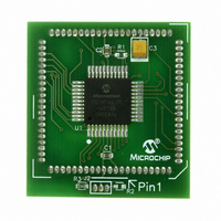
MODULE PLUG-IN PIC18F46J11 PIM
Manufacturer
Microchip Technology
Series
PIC®r
Datasheet
1.MA180023.pdf
(528 pages)
Specifications of MA180023
Accessory Type
Plug-In Module (PIM) - PIC18F46J11
Tool / Board Applications
General Purpose MCU, MPU, DSP, DSC
Mcu Supported Families
PIC18
Supported Devices
Stand-alone Or W/ HPC(DM183022) Or PIC18(DM183032)
Silicon Manufacturer
Microchip
Core Architecture
PIC
Core Sub-architecture
PIC18
Silicon Core Number
PIC18F
Silicon Family Name
PIC18FxxJxx
Lead Free Status / RoHS Status
Lead free / RoHS Compliant
For Use With/related Products
HPC Explorer Board (DM183022) or PIC18 Explorer Board (DM183032)
For Use With
DM183032 - BOARD EXPLORER PICDEM PIC18DM183022 - BOARD DEMO PIC18FXX22 64/80TQFP
Lead Free Status / RoHS Status
Lead free / RoHS Compliant
Available stocks
Company
Part Number
Manufacturer
Quantity
Price
Company:

Part Number:
MA180023
Manufacturer:
Microchip Technology
Quantity:
135


PIC18F46J11 FAMILY
SUBWFB
Syntax:
Operands:
Operation:
Status Affected:
Encoding:
Description:
Words:
Cycles:
Example 1:
Example 2:
Example 3:
DS39932C-page 444
Q Cycle Activity:
Before Instruction
After Instruction
Before Instruction
After Instruction
Before Instruction
After Instruction
Decode
REG
W
C
REG
W
C
Z
N
REG
W
C
REG
W
C
Z
N
REG
W
C
REG
W
C
Z
N
Q1
=
=
=
=
=
=
=
=
=
=
=
=
=
=
=
=
=
=
=
=
=
=
=
=
register ‘f’
(f) – (W) – (C) → dest
Subtract W from f with Borrow
SUBWFB
0 ≤ f ≤ 255
d ∈ [0,1]
a ∈ [0,1]
N, OV, C, DC, Z
Subtract W and the Carry flag (borrow)
from register ‘f’ (2’s complement
method). If ‘d’ is ‘0’, the result is stored
in W. If ‘d’ is ‘1’, the result is stored back
in register ‘f’ (default).
If ‘a’ is ‘0’, the Access Bank is selected.
If ‘a’ is ‘1’, the BSR is used to select the
GPR bank (default).
If ‘a’ is ‘0’ and the extended instruction
set is enabled, this instruction operates
in Indexed Literal Offset Addressing
mode whenever f ≤ 95 (5Fh). See
Section 26.2.3 “Byte-Oriented and
Bit-Oriented Instructions in Indexed
Literal Offset Mode” for details.
1
1
SUBWFB
SUBWFB REG, 0, 0
SUBWFB
Read
0101
Q2
19h
0Dh
1
0Ch
0Dh
1
0
0
1Bh
1Ah
0
1Bh
00h
1
1
0
03h
0Eh
1
F5h
0Eh
0
0
1
f {,d {,a}}
10da
REG, 1, 0
REG, 1, 0
(0001 1001)
(0000 1101)
(0000 1011)
(0000 1101)
; result is positive
(0001 1011)
(0001 1010)
(0001 1011)
; result is zero
(0000 0011)
(0000 1101)
(1111 0100)
; [2’s comp]
(0000 1101)
; result is negative
Process
Data
Q3
ffff
destination
Write to
Q4
ffff
SWAPF
Syntax:
Operands:
Operation:
Status Affected:
Encoding:
Description:
Words:
Cycles:
Example:
Q Cycle Activity:
Before Instruction
After Instruction
Decode
REG
REG
Q1
=
=
register ‘f’
Swap f
SWAPF f {,d {,a}}
0 ≤ f ≤ 255
d ∈ [0,1]
a ∈ [0,1]
(f<3:0>) → dest<7:4>,
(f<7:4>) → dest<3:0>
None
The upper and lower nibbles of register
‘f’ are exchanged. If ‘d’ is ‘0’, the result
is placed in W. If ‘d’ is ‘1’, the result is
placed in register ‘f’ (default).
If ‘a’ is ‘0’, the Access Bank is selected.
If ‘a’ is ‘1’, the BSR is used to select the
GPR bank (default).
If ‘a’ is ‘0’ and the extended instruction
set is enabled, this instruction operates
in Indexed Literal Offset Addressing
mode whenever f ≤ 95 (5Fh). See
Section 26.2.3 “Byte-Oriented and
Bit-Oriented Instructions in Indexed
Literal Offset Mode” for details.
1
1
SWAPF
Read
0011
Q2
53h
35h
© 2009 Microchip Technology Inc.
REG, 1, 0
10da
Process
Data
Q3
ffff
destination
Write to
Q4
ffff
Related parts for MA180023
Image
Part Number
Description
Manufacturer
Datasheet
Request
R

Part Number:
Description:
Manufacturer:
Microchip Technology Inc.
Datasheet:
Part Number:
Description:
Manufacturer:
Microchip Technology Inc.
Datasheet:
Part Number:
Description:
Manufacturer:
Microchip Technology Inc.
Datasheet:
Part Number:
Description:
Manufacturer:
Microchip Technology Inc.
Datasheet:
Part Number:
Description:
Manufacturer:
Microchip Technology Inc.
Datasheet:
Part Number:
Description:
Manufacturer:
Microchip Technology Inc.
Datasheet:
Part Number:
Description:
Manufacturer:
Microchip Technology Inc.
Datasheet:
Part Number:
Description:
Manufacturer:
Microchip Technology Inc.
Datasheet: