MA180023 Microchip Technology, MA180023 Datasheet - Page 403
MA180023
Manufacturer Part Number
MA180023
Description
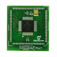
MODULE PLUG-IN PIC18F46J11 PIM
Manufacturer
Microchip Technology
Series
PIC®r
Datasheet
1.MA180023.pdf
(528 pages)
Specifications of MA180023
Accessory Type
Plug-In Module (PIM) - PIC18F46J11
Tool / Board Applications
General Purpose MCU, MPU, DSP, DSC
Mcu Supported Families
PIC18
Supported Devices
Stand-alone Or W/ HPC(DM183022) Or PIC18(DM183032)
Silicon Manufacturer
Microchip
Core Architecture
PIC
Core Sub-architecture
PIC18
Silicon Core Number
PIC18F
Silicon Family Name
PIC18FxxJxx
Lead Free Status / RoHS Status
Lead free / RoHS Compliant
For Use With/related Products
HPC Explorer Board (DM183022) or PIC18 Explorer Board (DM183032)
For Use With
DM183032 - BOARD EXPLORER PICDEM PIC18DM183022 - BOARD DEMO PIC18FXX22 64/80TQFP
Lead Free Status / RoHS Status
Lead free / RoHS Compliant
Available stocks
Company
Part Number
Manufacturer
Quantity
Price
Company:

Part Number:
MA180023
Manufacturer:
Microchip Technology
Quantity:
135


25.4
The Two-Speed Start-up feature helps to minimize the
latency period, from oscillator start-up to code execu-
tion, by allowing the microcontroller to use the INTRC
oscillator as a clock source until the primary clock
source is available. It is enabled by setting the IESO
Configuration bit.
Two-Speed Start-up should be enabled only if the
primary
(Crystal-Based) modes. Since the EC and ECPLL
modes do not require an Oscillator Start-up Timer
(OST) delay, Two-Speed Start-up should be disabled.
FIGURE 25-3:
25.4.1
While using the INTRC oscillator in Two-Speed
Start-up, the device still obeys the normal command
sequences for entering power-managed modes,
including
Section 3.1.4 “Multiple Sleep Commands”). In
practice, this means that user code can change the
SCS<1:0> bit settings or issue SLEEP instructions
before the OST times out. This would allow an applica-
tion to briefly wake-up, perform routine “housekeeping”
tasks and return to Sleep before the device starts to
operate from the primary oscillator.
User code can also check if the primary clock source is
currently providing the device clocking by checking the
status of the OSTS bit (OSCCON<3>). If the bit is set,
the primary oscillator is providing the clock. Otherwise,
the internal oscillator block is providing the clock during
wake-up from Reset or Sleep mode.
© 2009 Microchip Technology Inc.
Two-Speed Start-up
oscillator
SPECIAL CONSIDERATIONS FOR
USING TWO-SPEED START-UP
serial
Note1: T
CPU Clock
Peripheral
PLL Clock
Program
Counter
INTRC
Output
OSC1
Clock
SLEEP
OST
mode
TIMING TRANSITION FOR TWO-SPEED START-UP (INTRC TO HSPLL)
Wake from Interrupt Event
= 1024 T
PC
instructions
is
OSC
Q1
HS
; T
T
OST
PLL
(1)
or
= 2 ms (approx). These intervals are not shown to scale.
Q2
(refer
PC + 2
HSPLL
OSTS bit Set
T
Q3
PLL
to
(1)
Q4
PIC18F46J11 FAMILY
When enabled, Resets and wake-ups from Sleep mode
cause the device to configure itself to run from the inter-
nal oscillator block as the clock source, following the
time-out of the Power-up Timer after a Power-on Reset
is enabled. This allows almost immediate code
execution while the primary oscillator starts and the
OST is running. Once the OST times out, the device
automatically switches to PRI_RUN mode.
In all other power-managed modes, Two-Speed
Start-up is not used. The device will be clocked by the
currently selected clock source until the primary clock
source becomes available. The setting of the IESO bit
is ignored.
25.5
The Fail-Safe Clock Monitor (FSCM) allows the
microcontroller to continue operation in the event of an
external oscillator failure by automatically switching the
device clock to the internal oscillator block. The FSCM
function is enabled by setting the FCMEN Configuration
bit.
When FSCM is enabled, the INTRC oscillator runs at
all times to monitor clocks to peripherals and provide a
backup clock in the event of a clock failure. Clock
monitoring (shown in Figure 25-4) is accomplished by
creating a sample clock signal, which is the INTRC out-
put divided by 64. This allows ample time between
FSCM sample clocks for a peripheral clock edge to
occur. The peripheral device clock and the sample
clock are presented as inputs to the clock monitor latch.
The clock monitor is set on the falling edge of the
device clock source but cleared on the rising edge of
the sample clock.
Q1
1
Transition
2
Clock
Fail-Safe Clock Monitor
n-1 n
PC + 4
Q2
Q3 Q4
Q1
PC + 6
DS39932C-page 403
Q2
Q3
Related parts for MA180023
Image
Part Number
Description
Manufacturer
Datasheet
Request
R

Part Number:
Description:
Manufacturer:
Microchip Technology Inc.
Datasheet:
Part Number:
Description:
Manufacturer:
Microchip Technology Inc.
Datasheet:
Part Number:
Description:
Manufacturer:
Microchip Technology Inc.
Datasheet:
Part Number:
Description:
Manufacturer:
Microchip Technology Inc.
Datasheet:
Part Number:
Description:
Manufacturer:
Microchip Technology Inc.
Datasheet:
Part Number:
Description:
Manufacturer:
Microchip Technology Inc.
Datasheet:
Part Number:
Description:
Manufacturer:
Microchip Technology Inc.
Datasheet:
Part Number:
Description:
Manufacturer:
Microchip Technology Inc.
Datasheet: