MA180023 Microchip Technology, MA180023 Datasheet - Page 177
MA180023
Manufacturer Part Number
MA180023
Description
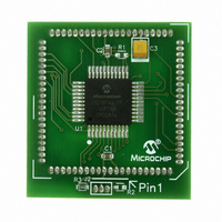
MODULE PLUG-IN PIC18F46J11 PIM
Manufacturer
Microchip Technology
Series
PIC®r
Datasheet
1.MA180023.pdf
(528 pages)
Specifications of MA180023
Accessory Type
Plug-In Module (PIM) - PIC18F46J11
Tool / Board Applications
General Purpose MCU, MPU, DSP, DSC
Mcu Supported Families
PIC18
Supported Devices
Stand-alone Or W/ HPC(DM183022) Or PIC18(DM183032)
Silicon Manufacturer
Microchip
Core Architecture
PIC
Core Sub-architecture
PIC18
Silicon Core Number
PIC18F
Silicon Family Name
PIC18FxxJxx
Lead Free Status / RoHS Status
Lead free / RoHS Compliant
For Use With/related Products
HPC Explorer Board (DM183022) or PIC18 Explorer Board (DM183032)
For Use With
DM183032 - BOARD EXPLORER PICDEM PIC18DM183022 - BOARD DEMO PIC18FXX22 64/80TQFP
Lead Free Status / RoHS Status
Lead free / RoHS Compliant
Available stocks
Company
Part Number
Manufacturer
Quantity
Price
Company:

Part Number:
MA180023
Manufacturer:
Microchip Technology
Quantity:
135


10.2.5
In the Addressable Parallel Slave Port mode
(
two extra inputs, PMA<1:0>, which are the address
lines 1 and 0. This makes the 4-byte buffer space
directly addressable as fixed pairs of read and write
buffers. As with Legacy Buffered mode, data is output
from PMDOUT1L, PMDOUT1H, PMDOUT2L and
PMDOUT2H, and is read in on PMDIN1L, PMDIN1H,
PMDIN2L and PMDIN2H. Table 10-1 provides the
buffer addressing for the incoming address to the input
and output registers.
FIGURE 10-6:
10.2.5.1
When chip select is active and a read strobe occurs
(PMCS = 1 and PMRD = 1), the data from one of the
four output bytes is presented onto PMD<7:0>. Which
byte is read depends on the 2-bit address placed on
ADDR<1:0>. Table 10-1 provides the corresponding
FIGURE 10-7:
© 2009 Microchip Technology Inc.
PMMODEH<1:0> = 01), the module is configured with
PMD<7:0>
PMA<1:0>
PMWR
Master
PMPIF
PMD<7:0>
PMA<1:0>
PMRD
PMCS
OBE
ADDRESSABLE PARALLEL SLAVE
PORT MODE
PMCS1
PMWR
PMRD
READ FROM SLAVE PORT
Address Bus
Data Bus
Control Lines
PARALLEL MASTER/SLAVE CONNECTION ADDRESSED BUFFER EXAMPLE
PARALLEL SLAVE PORT READ WAVEFORMS
PMD<7:0>
PMA<1:0>
PMCS
PMRD
PMWR
PIC18F46J11 FAMILY
TABLE 10-1:
output registers and their associated address. When an
output buffer is read, the corresponding OBxE bit is set.
The OBxE flag bit is set when all the buffers are empty.
If any buffer is already empty, OBxE = 1, the next read
to that buffer will generate an OBUF event.
Address
Decode
Write
PMA<1:0>
00
01
10
11
PIC18F Slave
PMDOUT1L (0)
PMDOUT1H (1)
PMDOUT2H (3)
PMDOUT2L (2)
|
Q4
SLAVE MODE BUFFER
ADDRESSING
PMDOUT2H((3)
PMDOUT1H (1)
PMDOUT1L (0)
PMDOUT2L (2)
|
Register
Q1
(Buffer)
Output
Address
Decode
Read
|
Q2
PMDIN1H (1)
PMDIN2H (3)
PMDIN1L (0)
PMDIN2L (2)
|
DS39932C-page 177
Q3
Input Register
PMDIN1H (1)
PMDIN2H (3)
PMDIN1L (0)
PMDIN2L (2)
(Buffer)
|
Q4
Related parts for MA180023
Image
Part Number
Description
Manufacturer
Datasheet
Request
R

Part Number:
Description:
Manufacturer:
Microchip Technology Inc.
Datasheet:
Part Number:
Description:
Manufacturer:
Microchip Technology Inc.
Datasheet:
Part Number:
Description:
Manufacturer:
Microchip Technology Inc.
Datasheet:
Part Number:
Description:
Manufacturer:
Microchip Technology Inc.
Datasheet:
Part Number:
Description:
Manufacturer:
Microchip Technology Inc.
Datasheet:
Part Number:
Description:
Manufacturer:
Microchip Technology Inc.
Datasheet:
Part Number:
Description:
Manufacturer:
Microchip Technology Inc.
Datasheet:
Part Number:
Description:
Manufacturer:
Microchip Technology Inc.
Datasheet: