MA180023 Microchip Technology, MA180023 Datasheet - Page 124
MA180023
Manufacturer Part Number
MA180023
Description
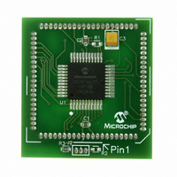
MODULE PLUG-IN PIC18F46J11 PIM
Manufacturer
Microchip Technology
Series
PIC®r
Datasheet
1.MA180023.pdf
(528 pages)
Specifications of MA180023
Accessory Type
Plug-In Module (PIM) - PIC18F46J11
Tool / Board Applications
General Purpose MCU, MPU, DSP, DSC
Mcu Supported Families
PIC18
Supported Devices
Stand-alone Or W/ HPC(DM183022) Or PIC18(DM183032)
Silicon Manufacturer
Microchip
Core Architecture
PIC
Core Sub-architecture
PIC18
Silicon Core Number
PIC18F
Silicon Family Name
PIC18FxxJxx
Lead Free Status / RoHS Status
Lead free / RoHS Compliant
For Use With/related Products
HPC Explorer Board (DM183022) or PIC18 Explorer Board (DM183032)
For Use With
DM183032 - BOARD EXPLORER PICDEM PIC18DM183022 - BOARD DEMO PIC18FXX22 64/80TQFP
Lead Free Status / RoHS Status
Lead free / RoHS Compliant
Available stocks
Company
Part Number
Manufacturer
Quantity
Price
Company:

Part Number:
MA180023
Manufacturer:
Microchip Technology
Quantity:
135


PIC18F46J11 FAMILY
8.6
External interrupts on the INT0, INT1, INT2 and INT3
pins are edge-triggered. If the corresponding INTEDGx
bit in the INTCON2 register is set (= 1), the interrupt is
triggered by a rising edge; if the bit is clear, the trigger
is on the falling edge. When a valid edge appears on
the INTx pin, the corresponding flag bit and INTxIF are
set. This interrupt can be disabled by clearing the
corresponding enable bit, INTxIE. Flag bit, INTxIF,
must be cleared in software in the Interrupt Service
Routine before re-enabling the interrupt.
All external interrupts (INT0, INT1, INT2 and INT3) can
wake-up the processor from the power-managed
modes if bit, INTxIE, was set prior to going into the
power-managed modes. If the Global Interrupt Enable
bit, GIE, is set, the processor will branch to the interrupt
vector following wake-up.
Interrupt priority for INT1, INT2 and INT3 is determined
by the value contained in the Interrupt Priority bits,
INT1IP (INTCON3<6>), INT2IP (INTCON3<7>) and
INT3IP (INTCON2<1>). There is no priority bit
associated with INT0. It is always a high-priority
interrupt source.
8.7
In 8-bit mode (which is the default), an overflow in the
TMR0 register (FFh → 00h) will set flag bit, TMR0IF. In
16-bit mode, an overflow in the TMR0H:TMR0L register
EXAMPLE 8-1:
DS39932C-page 124
MOVWF
MOVFF
MOVFF
;
; USER ISR CODE
;
MOVFF
MOVF
MOVFF
INTx Pin Interrupts
TMR0 Interrupt
W_TEMP
STATUS, STATUS_TEMP
BSR, BSR_TEMP
BSR_TEMP, BSR
W_TEMP, W
STATUS_TEMP, STATUS
SAVING STATUS, WREG AND BSR REGISTERS IN RAM
; W_TEMP is in virtual bank
; STATUS_TEMP located anywhere
; BSR_TMEP located anywhere
; Restore BSR
; Restore WREG
; Restore STATUS
module.
pair (FFFFh → 0000h) will set TMR0IF. The interrupt
can be enabled/disabled by setting/clearing enable bit,
TMR0IE (INTCON<5>). Interrupt priority for Timer0 is
determined by the value contained in the interrupt prior-
ity bit, TMR0IP (INTCON2<2>). See Section 11.0
“Timer0 Module” for further details on the Timer0
8.8
An input change on PORTB<7:4> sets flag bit, RBIF
(INTCON<0>). The interrupt can be enabled/disabled
by setting/clearing enable bit, RBIE (INTCON<3>).
Interrupt priority for PORTB interrupt-on-change is
determined by the value contained in the interrupt
priority bit, RBIP (INTCON2<0>).
8.9
During interrupts, the return PC address is saved on
the stack. Additionally, the WREG, STATUS and BSR
registers are saved on the Fast Return Stack. If a fast
return from interrupt is not used (see Section 5.3
“Data Memory Organization”), the user may need to
save the WREG, STATUS and BSR registers on entry
to the Interrupt Service Routine. Depending on the
user’s application, other registers may also need to be
saved. Example 8-1 saves and restores the WREG,
STATUS and BSR registers during an Interrupt Service
Routine.
PORTB Interrupt-on-Change
Context Saving During Interrupts
© 2009 Microchip Technology Inc.
Related parts for MA180023
Image
Part Number
Description
Manufacturer
Datasheet
Request
R

Part Number:
Description:
Manufacturer:
Microchip Technology Inc.
Datasheet:
Part Number:
Description:
Manufacturer:
Microchip Technology Inc.
Datasheet:
Part Number:
Description:
Manufacturer:
Microchip Technology Inc.
Datasheet:
Part Number:
Description:
Manufacturer:
Microchip Technology Inc.
Datasheet:
Part Number:
Description:
Manufacturer:
Microchip Technology Inc.
Datasheet:
Part Number:
Description:
Manufacturer:
Microchip Technology Inc.
Datasheet:
Part Number:
Description:
Manufacturer:
Microchip Technology Inc.
Datasheet:
Part Number:
Description:
Manufacturer:
Microchip Technology Inc.
Datasheet: