MA180023 Microchip Technology, MA180023 Datasheet - Page 267
MA180023
Manufacturer Part Number
MA180023
Description
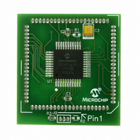
MODULE PLUG-IN PIC18F46J11 PIM
Manufacturer
Microchip Technology
Series
PIC®r
Datasheet
1.MA180023.pdf
(528 pages)
Specifications of MA180023
Accessory Type
Plug-In Module (PIM) - PIC18F46J11
Tool / Board Applications
General Purpose MCU, MPU, DSP, DSC
Mcu Supported Families
PIC18
Supported Devices
Stand-alone Or W/ HPC(DM183022) Or PIC18(DM183032)
Silicon Manufacturer
Microchip
Core Architecture
PIC
Core Sub-architecture
PIC18
Silicon Core Number
PIC18F
Silicon Family Name
PIC18FxxJxx
Lead Free Status / RoHS Status
Lead free / RoHS Compliant
For Use With/related Products
HPC Explorer Board (DM183022) or PIC18 Explorer Board (DM183032)
For Use With
DM183032 - BOARD EXPLORER PICDEM PIC18DM183022 - BOARD DEMO PIC18FXX22 64/80TQFP
Lead Free Status / RoHS Status
Lead free / RoHS Compliant
Available stocks
Company
Part Number
Manufacturer
Quantity
Price
Company:

Part Number:
MA180023
Manufacturer:
Microchip Technology
Quantity:
135


18.3.1
Each MSSP module has four registers for SPI mode
operation. These are:
• MSSPx Control Register 1 (SSPxCON1)
• MSSPx Status Register (SSPxSTAT)
• Serial Receive/Transmit Buffer Register
• MSSPx Shift Register (SSPxSR) – Not directly
SSPxCON1 and SSPxSTAT are the control and status
registers in SPI mode operation. The SSPxCON1
register is readable and writable. The lower six bits of
the SSPxSTAT are read-only. The upper two bits of the
SSPxSTAT are read/write.
REGISTER 18-1:
© 2009 Microchip Technology Inc.
bit 7
Legend:
R = Readable bit
-n = Value at POR
bit 7
bit 6
bit 5
bit 4
bit 3
bit 2
bit 1
bit 0
Note 1:
(SSPxBUF)
accessible
R/W-1
SMP
Polarity of clock state is set by the CKP bit (SSPxCON1<4>).
REGISTERS
SMP: Sample bit
SPI Master mode:
1 = Input data sampled at end of data output time
0 = Input data sampled at middle of data output time
SPI Slave mode:
SMP must be cleared when SPI is used in Slave mode.
CKE: SPI Clock Select bit
1 = Transmit occurs on transition from active to Idle clock state
0 = Transmit occurs on transition from Idle to active clock state
D/A: Data/Address bit
Used in I
P: Stop bit
Used in I
S: Start bit
Used in I
R/W: Read/Write Information bit
Used in I
UA: Update Address bit
Used in I
BF: Buffer Full Status bit
1 = Receive complete, SSPxBUF is full
0 = Receive not complete, SSPxBUF is empty
CKE
R/W-1
SSPxSTAT: MSSPx STATUS REGISTER – SPI MODE (ACCESS FC7h/F73h)
(1)
2
2
2
2
2
C™ mode only.
C mode only; this bit is cleared when the MSSP module is disabled, SSPEN is cleared.
C mode only.
C mode only.
C mode only.
W = Writable bit
‘1’ = Bit is set
D/A
R-1
(1)
R-1
P
U = Unimplemented bit, read as ‘0’
‘0’ = Bit is cleared
PIC18F46J11 FAMILY
SSPxSR is the shift register used for shifting data in or
out. SSPxBUF is the buffer register to which data
bytes are written to or read from.
In receive operations, SSPxSR and SSPxBUF
together create a double-buffered receiver. When
SSPxSR receives a complete byte, it is transferred to
SSPxBUF and the SSPxIF interrupt is set.
During
double-buffered. A write to SSPxBUF will write to both
SSPxBUF and SSPxSR.
R-1
S
transmission,
R/W
R-1
x = Bit is unknown
the
R-1
UA
SSPxBUF
DS39932C-page 267
R-1
BF
is
bit 0
not
Related parts for MA180023
Image
Part Number
Description
Manufacturer
Datasheet
Request
R

Part Number:
Description:
Manufacturer:
Microchip Technology Inc.
Datasheet:
Part Number:
Description:
Manufacturer:
Microchip Technology Inc.
Datasheet:
Part Number:
Description:
Manufacturer:
Microchip Technology Inc.
Datasheet:
Part Number:
Description:
Manufacturer:
Microchip Technology Inc.
Datasheet:
Part Number:
Description:
Manufacturer:
Microchip Technology Inc.
Datasheet:
Part Number:
Description:
Manufacturer:
Microchip Technology Inc.
Datasheet:
Part Number:
Description:
Manufacturer:
Microchip Technology Inc.
Datasheet:
Part Number:
Description:
Manufacturer:
Microchip Technology Inc.
Datasheet: