MA180023 Microchip Technology, MA180023 Datasheet - Page 515
MA180023
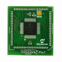
Manufacturer Part Number
MA180023
Description
MODULE PLUG-IN PIC18F46J11 PIM
Manufacturer
Microchip Technology
Series
PIC®r
Datasheet
1.MA180023.pdf
(528 pages)
Specifications of MA180023
Accessory Type
Plug-In Module (PIM) - PIC18F46J11
Tool / Board Applications
General Purpose MCU, MPU, DSP, DSC
Mcu Supported Families
PIC18
Supported Devices
Stand-alone Or W/ HPC(DM183022) Or PIC18(DM183032)
Silicon Manufacturer
Microchip
Core Architecture
PIC
Core Sub-architecture
PIC18
Silicon Core Number
PIC18F
Silicon Family Name
PIC18FxxJxx
Lead Free Status / RoHS Status
Lead free / RoHS Compliant
For Use With/related Products
HPC Explorer Board (DM183022) or PIC18 Explorer Board (DM183032)
For Use With
DM183032 - BOARD EXPLORER PICDEM PIC18DM183022 - BOARD DEMO PIC18FXX22 64/80TQFP
Lead Free Status / RoHS Status
Lead free / RoHS Compliant
Available stocks
Company
Part Number
Manufacturer
Quantity
Price
Company:

Part Number:
MA180023
Manufacturer:
Microchip Technology
Quantity:
135


Data Memory ..................................................................... 78
DAW ................................................................................. 426
DC Characteristics ........................................................... 474
DCFSNZ .......................................................................... 427
DECF ............................................................................... 426
DECFSZ ........................................................................... 427
Development Support ...................................................... 457
Device Differences ........................................................... 511
Device Overview ................................................................ 11
Direct Addressing ............................................................... 91
E
Effect on Standard PIC MCU Instructions ........................ 454
Electrical Characteristics .................................................. 461
Enhanced Capture/Compare/PWM (ECCP) .................... 241
Enhanced Universal Synchronous Asynchronous Receiver
Equations
Errata ................................................................................... 9
EUSART .......................................................................... 321
© 2009 Microchip Technology Inc.
Indirect ....................................................................... 90
Inherent and Literal .................................................... 90
Access Bank .............................................................. 80
Extended Instruction Set ............................................ 92
General Purpose Registers ........................................ 80
Memory Maps
Special Function Registers ........................................ 81
Power-Down and Supply Current ............................ 464
Supply Voltage ......................................................... 463
Details on Individual Family Members ....................... 12
Features (28-Pin Devices) ......................................... 13
Features (44-Pin Devices) ......................................... 13
Other Special Features .............................................. 12
Absolute Maximum Ratings ..................................... 461
Associated Registers ............................................... 263
Capture Mode. See Capture.
Compare Mode. See Compare.
ECCP Mode and Timer Resources .......................... 243
Enhanced PWM Mode ............................................. 249
Outputs and Configuration ....................................... 243
Transmitter (EUSART). See EUSART.
A/D Acquisition Time ................................................ 350
A/D Minimum Charging Time ................................... 350
Bytes Transmitted for a Given DMABC ................... 281
Calculating the Minimum Required Acquisition Time .....
Asynchronous Mode ................................................ 331
Access Bank Special Function Registers .......... 81
Non-Access Bank Special Function Registers .. 82
PIC18F46J11 Family Devices ........................... 79
Context Defined SFRs ....................................... 83
Auto-Restart ..................................................... 258
Auto-Shutdown ................................................ 257
Direction Change in Full-Bridge Output Mode . 255
Full-Bridge Application ..................................... 253
Full-Bridge Mode ............................................. 253
Half-Bridge Application .................................... 252
Half-Bridge Application Examples ................... 259
Half-Bridge Mode ............................................. 252
Output Relationships (Active-High) .................. 250
Output Relationships Diagram (Active-Low) .... 251
Programmable Dead-Band Delay .................... 259
Shoot-Through Current .................................... 259
Start-up Considerations ................................... 256
350
12-Bit Break Transmit and Receive ................. 336
Associated Registers, Reception ..................... 334
Associated Registers, Transmission ................ 332
PIC18F46J11 FAMILY
Extended Instruction Set
Extended Instructions
External Clock Input ........................................................... 34
F
Fail-Safe Clock Monitor ........................................... 389, 403
Fast Register Stack ........................................................... 75
Features Overview ............................................................... 3
Firmware Instructions ...................................................... 407
Flash Program Memory ..................................................... 97
FSCM. See Fail-Safe Clock Monitor.
Baud Rate Generator
Baud Rate Generator (BRG) ................................... 325
Synchronous Master Mode ...................................... 337
Synchronous Slave Mode ........................................ 341
ADDFSR .................................................................. 450
ADDULNK ............................................................... 450
CALLW .................................................................... 451
MOVSF .................................................................... 451
MOVSS .................................................................... 452
PUSHL ..................................................................... 452
SUBFSR .................................................................. 453
SUBULNK ................................................................ 453
Considerations when Enabling ................................ 454
Interrupts in Power-Managed Modes ...................... 405
POR or Wake-up From Sleep .................................. 405
WDT During Oscillator Failure ................................. 404
Comparative Table ...................................................... 4
Associated Registers ............................................... 106
Control Registers ....................................................... 98
Erase Sequence ...................................................... 102
Erasing .................................................................... 102
Operation During Code-Protect ............................... 106
Reading ................................................................... 101
Table Pointer
Table Pointer Boundaries ........................................ 100
Table Reads and Table Writes .................................. 97
Write Sequence ....................................................... 103
Write Sequence (Word Programming) .................... 105
Writing ..................................................................... 103
Auto-Wake-up on Sync Break ......................... 334
Receiver .......................................................... 333
Setting Up 9-Bit Mode with Address Detect .... 333
Transmitter ...................................................... 331
Operation in Power-Managed Mode ................ 325
Associated Registers ....................................... 326
Auto-Baud Rate Detect .................................... 329
Baud Rates, Asynchronous Modes ................. 327
Formulas .......................................................... 325
High Baud Rate Select (BRGH Bit) ................. 325
Sampling ......................................................... 325
Associated Registers, Reception ..................... 340
Associated Registers, Transmission ............... 338
Reception ........................................................ 339
Transmission ................................................... 337
Associated Registers, Reception ..................... 343
Associated Registers, Transmission ............... 342
Reception ........................................................ 343
Transmission ................................................... 341
EECON1 and EECON2 ..................................... 98
TABLAT (Table Latch) ..................................... 100
TBLPTR (Table Pointer) Register .................... 100
Boundaries Based on Operation ..................... 100
Unexpected Termination ................................. 106
Write Verify ...................................................... 106
DS39932C-page 515
Related parts for MA180023
Image
Part Number
Description
Manufacturer
Datasheet
Request
R

Part Number:
Description:
Manufacturer:
Microchip Technology Inc.
Datasheet:
Part Number:
Description:
Manufacturer:
Microchip Technology Inc.
Datasheet:
Part Number:
Description:
Manufacturer:
Microchip Technology Inc.
Datasheet:
Part Number:
Description:
Manufacturer:
Microchip Technology Inc.
Datasheet:
Part Number:
Description:
Manufacturer:
Microchip Technology Inc.
Datasheet:
Part Number:
Description:
Manufacturer:
Microchip Technology Inc.
Datasheet:
Part Number:
Description:
Manufacturer:
Microchip Technology Inc.
Datasheet:
Part Number:
Description:
Manufacturer:
Microchip Technology Inc.
Datasheet: