MA180023 Microchip Technology, MA180023 Datasheet - Page 285
MA180023
Manufacturer Part Number
MA180023
Description
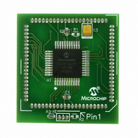
MODULE PLUG-IN PIC18F46J11 PIM
Manufacturer
Microchip Technology
Series
PIC®r
Datasheet
1.MA180023.pdf
(528 pages)
Specifications of MA180023
Accessory Type
Plug-In Module (PIM) - PIC18F46J11
Tool / Board Applications
General Purpose MCU, MPU, DSP, DSC
Mcu Supported Families
PIC18
Supported Devices
Stand-alone Or W/ HPC(DM183022) Or PIC18(DM183032)
Silicon Manufacturer
Microchip
Core Architecture
PIC
Core Sub-architecture
PIC18
Silicon Core Number
PIC18F
Silicon Family Name
PIC18FxxJxx
Lead Free Status / RoHS Status
Lead free / RoHS Compliant
For Use With/related Products
HPC Explorer Board (DM183022) or PIC18 Explorer Board (DM183032)
For Use With
DM183032 - BOARD EXPLORER PICDEM PIC18DM183022 - BOARD DEMO PIC18FXX22 64/80TQFP
Lead Free Status / RoHS Status
Lead free / RoHS Compliant
Available stocks
Company
Part Number
Manufacturer
Quantity
Price
Company:

Part Number:
MA180023
Manufacturer:
Microchip Technology
Quantity:
135


18.5
The MSSP module in I
master and slave functions (including general call
support), and provides interrupts on Start and Stop bits
in hardware to determine a free bus (multi-master
function). The MSSP module implements the standard
mode specifications and 7-bit and 10-bit addressing.
Two pins are used for data transfer:
• Serial Clock (SCLx) –
• Serial Data (SDAx) –
The user must configure these pins as inputs by setting
the associated TRIS bits.
FIGURE 18-7:
© 2009 Microchip Technology Inc.
Note:
SDAx
SCLx
RB4/PMA1/KBI0/SCK1/SCL1/RP7 or
RD0/PMD0/SCL2
RB5/PMA0/KBI1/SDI1/SDA1/RP8 or
RD1/PMD1/SDA2
Only port I/O names are used in this diagram for
the sake of brevity. Refer to the text for a full list of
multiplexed functions.
I
2
C Mode
Read
Shift
Clock
MSb
SSPxADD reg
Address Mask
Stop bit Detect
Match Detect
SSPxBUF reg
SSPxSR reg
MSSPx BLOCK DIAGRAM
(I
Start and
2
2
C mode fully implements all
C™ MODE)
LSb
Write
Addr Match
Set, Reset
S, P bits
(SSPxSTAT reg)
Internal
Data Bus
PIC18F46J11 FAMILY
18.5.1
The MSSP module has six registers for I
These are:
• MSSPx Control Register 1 (SSPxCON1)
• MSSPx Control Register 2 (SSPxCON2)
• MSSPx Status Register (SSPxSTAT)
• Serial Receive/Transmit Buffer Register
• MSSPx Shift Register (SSPxSR) – Not directly
• MSSPx Address Register (SSPxADD)
• MSSPx 7-Bit Address Mask Register (SSPxMSK)
SSPxCON1, SSPxCON2 and SSPxSTAT are the
control and status registers in I
SSPxCON1 and SSPxCON2 registers are readable and
writable. The lower six bits of the SSPxSTAT are
read-only. The upper two bits of the SSPxSTAT are
read/write.
SSPxSR is the shift register used for shifting data in or
out. SSPxBUF is the buffer register to which data
bytes are written to or read from.
SSPxADD contains the slave device address when the
MSSP is configured in I
MSSP is configured in Master mode, the lower seven
bits of SSPxADD act as the Baud Rate Generator
(BRG) reload value.
SSPxMSK holds the slave address mask value when
the module is configured for 7-Bit Address Masking
mode. While it is a separate register, it shares the same
SFR address as SSPxADD; it is only accessible when
the SSPM<3:0> bits are specifically set to permit
access.
Section 18.5.3.4 “7-Bit Address Masking Mode”.
In receive operations, SSPxSR and SSPxBUF
together, create a double-buffered receiver. When
SSPxSR receives a complete byte, it is transferred to
SSPxBUF and the SSPxIF interrupt is set.
During
double-buffered. A write to SSPxBUF will write to both
SSPxBUF and SSPxSR.
(SSPxBUF)
accessible
transmission,
Additional
REGISTERS
details
2
the
C Slave mode. When the
2
C mode operation. The
SSPxBUF
are
DS39932C-page 285
provided
2
C operation.
is
not
in
Related parts for MA180023
Image
Part Number
Description
Manufacturer
Datasheet
Request
R

Part Number:
Description:
Manufacturer:
Microchip Technology Inc.
Datasheet:
Part Number:
Description:
Manufacturer:
Microchip Technology Inc.
Datasheet:
Part Number:
Description:
Manufacturer:
Microchip Technology Inc.
Datasheet:
Part Number:
Description:
Manufacturer:
Microchip Technology Inc.
Datasheet:
Part Number:
Description:
Manufacturer:
Microchip Technology Inc.
Datasheet:
Part Number:
Description:
Manufacturer:
Microchip Technology Inc.
Datasheet:
Part Number:
Description:
Manufacturer:
Microchip Technology Inc.
Datasheet:
Part Number:
Description:
Manufacturer:
Microchip Technology Inc.
Datasheet: