MA180023 Microchip Technology, MA180023 Datasheet - Page 279
MA180023
Manufacturer Part Number
MA180023
Description
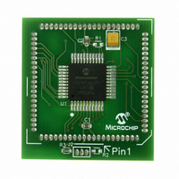
MODULE PLUG-IN PIC18F46J11 PIM
Manufacturer
Microchip Technology
Series
PIC®r
Datasheet
1.MA180023.pdf
(528 pages)
Specifications of MA180023
Accessory Type
Plug-In Module (PIM) - PIC18F46J11
Tool / Board Applications
General Purpose MCU, MPU, DSP, DSC
Mcu Supported Families
PIC18
Supported Devices
Stand-alone Or W/ HPC(DM183022) Or PIC18(DM183032)
Silicon Manufacturer
Microchip
Core Architecture
PIC
Core Sub-architecture
PIC18
Silicon Core Number
PIC18F
Silicon Family Name
PIC18FxxJxx
Lead Free Status / RoHS Status
Lead free / RoHS Compliant
For Use With/related Products
HPC Explorer Board (DM183022) or PIC18 Explorer Board (DM183032)
For Use With
DM183032 - BOARD EXPLORER PICDEM PIC18DM183022 - BOARD DEMO PIC18FXX22 64/80TQFP
Lead Free Status / RoHS Status
Lead free / RoHS Compliant
Available stocks
Company
Part Number
Manufacturer
Quantity
Price
Company:

Part Number:
MA180023
Manufacturer:
Microchip Technology
Quantity:
135


18.4.4.2
The DMACON2 register contains control bits for
controlling interrupt generation and inter-byte delay
behavior. The INTLVL<3:0> bits are used to select when
an SSP2IF interrupt should be generated.The function
of the DLYCYC<3:0> bits depends on the SPI operating
mode (Master/Slave), as well as the DLYINTEN setting.
In SPI Master mode, the DLYCYC<3:0> bits can be used
REGISTER 18-4:
© 2009 Microchip Technology Inc.
bit 7
Legend:
R = Readable bit
-n = Value at POR
bit 7-4
DLYCYC3
R/W-0
DMACON2
DLYCYC<3:0>: Delay Cycle Selection bits
When DLYINTEN = 0, these bits specify the additional delay (above the base overhead of the
hardware) in number of T
When DLYINTEN = 1, these bits specify the additional delay in number of T
completed transfer before an interrupt to the CPU is invoked. In this case, the delay before the
SSP2BUF register is written again is 1 T
1111 = Delay time in number of instruction cycles is 2,048 cycles
1110 = Delay time in number of instruction cycles is 1,024 cycles
1101 = Delay time in number of instruction cycles is 896 cycles
1100 = Delay time in number of instruction cycles is 768 cycles
1011 = Delay time in number of instruction cycles is 640 cycles
1010 = Delay time in number of instruction cycles is 512 cycles
1001 = Delay time in number of instruction cycles is 384 cycles
1000 = Delay time in number of instruction cycles is 256 cycles
0111 = Delay time in number of instruction cycles is 128 cycles
0110 = Delay time in number of instruction cycles is 64 cycles
0101 = Delay time in number of instruction cycles is 32 cycles
0100 = Delay time in number of instruction cycles is 16 cycles
0011 = Delay time in number of instruction cycles is 8 cycles
0010 = Delay time in number of instruction cycles is 4 cycles
0001 = Delay time in number of instruction cycles is 2 cycles
0000 = Delay time in number of instruction cycles is 1 cycle
DLYCYC2
R/W-0
DMACON2: DMA CONTROL REGISTER 2 (ACCESS F86h)
W = Writable bit
‘1’ = Bit is set
DLYCYC1
R/W-0
CY
cycles before the SSP2BUF register is written again for the next transfer.
DLYCYC0
R/W-0
CY
U = Unimplemented bit, read as ‘0’
‘0’ = Bit is cleared
+ (base overhead of hardware).
INTLVL3
PIC18F46J11 FAMILY
R/W-0
to control how much time the module will Idle between
bytes in a transfer. By default, the hardware requires a
minimum delay of: 8 T
and 15 T
added with the DLYCYC bits. In SPI Slave modes, the
DLYCYC<3:0> bits may optionally be used to trigger an
additional time-out based interrupt.
CY
INTLVL2
for F
R/W-0
OSC
CY
/64. Additional delays can be
for F
x = Bit is unknown
INTLVL1
CY
R/W-0
OSC
cycles from the latest
/4, 9 T
DS39932C-page 279
CY
for F
INTLVL0
R/W-0
OSC
bit 0
/16
Related parts for MA180023
Image
Part Number
Description
Manufacturer
Datasheet
Request
R

Part Number:
Description:
Manufacturer:
Microchip Technology Inc.
Datasheet:
Part Number:
Description:
Manufacturer:
Microchip Technology Inc.
Datasheet:
Part Number:
Description:
Manufacturer:
Microchip Technology Inc.
Datasheet:
Part Number:
Description:
Manufacturer:
Microchip Technology Inc.
Datasheet:
Part Number:
Description:
Manufacturer:
Microchip Technology Inc.
Datasheet:
Part Number:
Description:
Manufacturer:
Microchip Technology Inc.
Datasheet:
Part Number:
Description:
Manufacturer:
Microchip Technology Inc.
Datasheet:
Part Number:
Description:
Manufacturer:
Microchip Technology Inc.
Datasheet: