MA180023 Microchip Technology, MA180023 Datasheet - Page 169
MA180023
Manufacturer Part Number
MA180023
Description
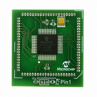
MODULE PLUG-IN PIC18F46J11 PIM
Manufacturer
Microchip Technology
Series
PIC®r
Datasheet
1.MA180023.pdf
(528 pages)
Specifications of MA180023
Accessory Type
Plug-In Module (PIM) - PIC18F46J11
Tool / Board Applications
General Purpose MCU, MPU, DSP, DSC
Mcu Supported Families
PIC18
Supported Devices
Stand-alone Or W/ HPC(DM183022) Or PIC18(DM183032)
Silicon Manufacturer
Microchip
Core Architecture
PIC
Core Sub-architecture
PIC18
Silicon Core Number
PIC18F
Silicon Family Name
PIC18FxxJxx
Lead Free Status / RoHS Status
Lead free / RoHS Compliant
For Use With/related Products
HPC Explorer Board (DM183022) or PIC18 Explorer Board (DM183032)
For Use With
DM183032 - BOARD EXPLORER PICDEM PIC18DM183022 - BOARD DEMO PIC18FXX22 64/80TQFP
Lead Free Status / RoHS Status
Lead free / RoHS Compliant
Available stocks
Company
Part Number
Manufacturer
Quantity
Price
Company:

Part Number:
MA180023
Manufacturer:
Microchip Technology
Quantity:
135


REGISTER 10-4:
© 2009 Microchip Technology Inc.
bit 7
Legend:
R = Readable bit
-n = Value at POR
bit 7-6
bit 5-2
bit 1-0
Note 1:
WAITB1
R/W-0
2:
(2)
This register is only available in 44-pin devices.
WAITBx and WAITEx bits are ignored whenever WAITM<3:0> = 0000.
WAITB<1:0>: Data Setup to Read/Write Wait State Configuration bits
11 = Data wait of 4 T
10 = Data wait of 3 T
01 = Data wait of 2 T
00 = Data wait of 1 T
WAITM<3:0>: Read to Byte Enable Strobe Wait State Configuration bits
1111 = Wait of additional 15 T
.
.
.
0001 = Wait of additional 1 T
0000 = No additional Wait cycles (operation forced into one T
WAITE<1:0>: Data Hold After Strobe Wait State Configuration bits
11 = Wait of 4 T
10 = Wait of 3 T
01 = Wait of 2 T
00 = Wait of 1 T
WAITB0
R/W-0
PMMODEL: PARALLEL PORT MODE REGISTER LOW BYTE (BANKED F5Ch)
(2)
W = Writable bit
‘1’ = Bit is set
CY
CY
CY
CY
WAITM3
R/W-0
CY
CY
CY
CY
; multiplexed address phase of 4 T
; multiplexed address phase of 3 T
; multiplexed address phase of 2 T
; multiplexed address phase of 1 T
CY
CY
WAITM2
R/W-0
U = Unimplemented bit, read as ‘0’
‘0’ = Bit is cleared
PIC18F46J11 FAMILY
WAITM1
R/W-0
CY
CY
CY
CY
WAITM0
CY
R/W-0
)
(2)
(2)
x = Bit is unknown
WAITE1
R/W-0
(2)
DS39932C-page 169
WAITE0
R/W-0
bit 0
(2)
(1)
Related parts for MA180023
Image
Part Number
Description
Manufacturer
Datasheet
Request
R

Part Number:
Description:
Manufacturer:
Microchip Technology Inc.
Datasheet:
Part Number:
Description:
Manufacturer:
Microchip Technology Inc.
Datasheet:
Part Number:
Description:
Manufacturer:
Microchip Technology Inc.
Datasheet:
Part Number:
Description:
Manufacturer:
Microchip Technology Inc.
Datasheet:
Part Number:
Description:
Manufacturer:
Microchip Technology Inc.
Datasheet:
Part Number:
Description:
Manufacturer:
Microchip Technology Inc.
Datasheet:
Part Number:
Description:
Manufacturer:
Microchip Technology Inc.
Datasheet:
Part Number:
Description:
Manufacturer:
Microchip Technology Inc.
Datasheet: