MA180023 Microchip Technology, MA180023 Datasheet - Page 305
MA180023
Manufacturer Part Number
MA180023
Description
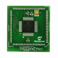
MODULE PLUG-IN PIC18F46J11 PIM
Manufacturer
Microchip Technology
Series
PIC®r
Datasheet
1.MA180023.pdf
(528 pages)
Specifications of MA180023
Accessory Type
Plug-In Module (PIM) - PIC18F46J11
Tool / Board Applications
General Purpose MCU, MPU, DSP, DSC
Mcu Supported Families
PIC18
Supported Devices
Stand-alone Or W/ HPC(DM183022) Or PIC18(DM183032)
Silicon Manufacturer
Microchip
Core Architecture
PIC
Core Sub-architecture
PIC18
Silicon Core Number
PIC18F
Silicon Family Name
PIC18FxxJxx
Lead Free Status / RoHS Status
Lead free / RoHS Compliant
For Use With/related Products
HPC Explorer Board (DM183022) or PIC18 Explorer Board (DM183032)
For Use With
DM183032 - BOARD EXPLORER PICDEM PIC18DM183022 - BOARD DEMO PIC18FXX22 64/80TQFP
Lead Free Status / RoHS Status
Lead free / RoHS Compliant
Available stocks
Company
Part Number
Manufacturer
Quantity
Price
Company:

Part Number:
MA180023
Manufacturer:
Microchip Technology
Quantity:
135


FIGURE 18-18:
18.5.6.1
The master device generates all of the serial clock
pulses and the Start and Stop conditions. A transfer is
ended with a Stop condition or with a Repeated Start
condition. Since the Repeated Start condition is also
the beginning of the next serial transfer, the I
not be released.
In Master Transmitter mode, serial data is output
through SDAx while SCLx outputs the serial clock. The
first byte transmitted contains the slave address of the
receiving device (7 bits) and the Read/Write (R/W) bit.
In this case, the R/W bit will be logic ‘0’. Serial data is
transmitted 8 bits at a time. After each byte is transmit-
ted, an Acknowledge bit is received. S and P conditions
are output to indicate the beginning and the end of a
serial transfer.
© 2009 Microchip Technology Inc.
Note:
SDAx
SCLx
The MSSP module, when configured in
I
of events. For instance, the user is not
allowed to initiate a Start condition and
immediately write the SSPxBUF register to
initiate transmission before the Start
condition is complete. In this case, the
SSPxBUF will not be written to and the
WCOL bit will be set, indicating that a write
to the SSPxBUF did not occur.
2
C Master mode, does not allow queueing
I
2
C Master Mode Operation
MSSPx BLOCK DIAGRAM (I
SDAx In
Bus Collision
SCLx In
Read
2
MSb
C bus will
Write Collision Detect
Start bit, Stop bit,
End of XMIT/RCV
State Counter for
Clock Arbitration
Acknowledge
Stop bit Detect
Start bit Detect
SSPxBUF
SSPxSR
Generate
2
C™ MASTER MODE)
LSb
PIC18F46J11 FAMILY
Write
The following events will cause the MSSP Interrupt
Flag bit, SSPxIF, to be set (and MSSP interrupt, if
enabled):
• Start condition
• Stop condition
• Data transfer byte transmitted/received
• Acknowledge transmitted
• Repeated Start
In Master Receive mode, the first byte transmitted
contains the slave address of the transmitting device
(7 bits) and the R/W bit. In this case, the R/W bit will be
logic ‘1’. Thus, the first byte transmitted is a 7-bit slave
address, followed by a ‘1’ to indicate the receive bit.
Serial data is received via SDAx, while SCLx outputs
the serial clock. Serial data is received 8 bits at a time.
After each byte is received, an Acknowledge bit is
transmitted. S and P conditions indicate the beginning
and end of transmission.
The BRG, used for the SPI mode operation, is used to
set the SCLx clock frequency for either 100 kHz,
400 kHz or 1 MHz I
“Baud Rate” for more details.
Clock
Data Bus
Shift
Internal
Set/Reset S, P (SSPxSTAT), WCOL (SSPxCON1)
Set SSPxIF, BCLxIF
Reset ACKSTAT, PEN (SSPxCON2)
2
C operation. See Section 18.5.7
SSPxADD<6:0>
SSPM<3:0>
Generator
Baud
Rate
DS39932C-page 305
Related parts for MA180023
Image
Part Number
Description
Manufacturer
Datasheet
Request
R

Part Number:
Description:
Manufacturer:
Microchip Technology Inc.
Datasheet:
Part Number:
Description:
Manufacturer:
Microchip Technology Inc.
Datasheet:
Part Number:
Description:
Manufacturer:
Microchip Technology Inc.
Datasheet:
Part Number:
Description:
Manufacturer:
Microchip Technology Inc.
Datasheet:
Part Number:
Description:
Manufacturer:
Microchip Technology Inc.
Datasheet:
Part Number:
Description:
Manufacturer:
Microchip Technology Inc.
Datasheet:
Part Number:
Description:
Manufacturer:
Microchip Technology Inc.
Datasheet:
Part Number:
Description:
Manufacturer:
Microchip Technology Inc.
Datasheet: