MA180023 Microchip Technology, MA180023 Datasheet - Page 349
MA180023
Manufacturer Part Number
MA180023
Description
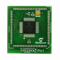
MODULE PLUG-IN PIC18F46J11 PIM
Manufacturer
Microchip Technology
Series
PIC®r
Datasheet
1.MA180023.pdf
(528 pages)
Specifications of MA180023
Accessory Type
Plug-In Module (PIM) - PIC18F46J11
Tool / Board Applications
General Purpose MCU, MPU, DSP, DSC
Mcu Supported Families
PIC18
Supported Devices
Stand-alone Or W/ HPC(DM183022) Or PIC18(DM183032)
Silicon Manufacturer
Microchip
Core Architecture
PIC
Core Sub-architecture
PIC18
Silicon Core Number
PIC18F
Silicon Family Name
PIC18FxxJxx
Lead Free Status / RoHS Status
Lead free / RoHS Compliant
For Use With/related Products
HPC Explorer Board (DM183022) or PIC18 Explorer Board (DM183032)
For Use With
DM183032 - BOARD EXPLORER PICDEM PIC18DM183022 - BOARD DEMO PIC18FXX22 64/80TQFP
Lead Free Status / RoHS Status
Lead free / RoHS Compliant
Available stocks
Company
Part Number
Manufacturer
Quantity
Price
Company:

Part Number:
MA180023
Manufacturer:
Microchip Technology
Quantity:
135


After the A/D module has been configured as desired,
the selected channel must be acquired before the
conversion is started. The analog input channels must
have their corresponding TRIS bits selected as an
input. To determine acquisition time, see Section 20.1
“A/D Acquisition Requirements”. After this acquisi-
tion time has elapsed, the A/D conversion can be
started. An acquisition time can be programmed to
occur between setting the GO/DONE bit and the actual
start of the conversion.
The following steps should be followed to do an A/D
conversion:
1.
FIGURE 20-2:
© 2009 Microchip Technology Inc.
Configure the A/D module:
• Configure the required ADC pins as analog
• Set voltage reference using ADCON0
• Select A/D input channel (ADCON0)
• Select A/D acquisition time (ADCON1)
• Select A/D conversion clock (ADCON1)
• Turn on A/D module (ADCON0)
pins using ANCON0, ANCON1
Legend: C
V
AIN
R
S
V
I
R
SS
C
R
LEAKAGE
T
PIN
IC
HOLD
SS
ANALOG INPUT MODEL
ANx
C
5 pF
PIN
= Input Capacitance
= Threshold Voltage
= Leakage Current at the pin due to
= Interconnect Resistance
= Sampling Switch
= Sample/Hold Capacitance (from DAC)
= Sampling Switch Resistance
various junctions
V
DD
V
V
T
T
= 0.6V
= 0.6V
I
±100 nA
PIC18F46J11 FAMILY
LEAKAGE
2.
3.
4.
5.
6.
7.
R
IC
Configure A/D interrupt (if desired):
• Clear ADIF bit
• Set ADIE bit
• Set GIE bit
Wait the required acquisition time (if required).
Start conversion:
• Set GO/DONE bit (ADCON0<1>)
Wait for A/D conversion to complete, by either:
• Polling for the GO/DONE bit to be cleared
OR
• Waiting for the A/D interrupt
Read A/D Result registers (ADRESH:ADRESL);
clear bit, ADIF, if required.
For next conversion, go to step 1 or step 2, as
required. The A/D conversion time per bit is
defined as T
required before next acquisition starts.
≤ 1k
SS
Sampling
Switch
V
DD
AD
R
SS
. A minimum wait of 2 T
Sampling Switch
1
V
SS
C
2
HOLD
3
DS39932C-page 349
= 25 pF
(kΩ)
4
AD
is
Related parts for MA180023
Image
Part Number
Description
Manufacturer
Datasheet
Request
R

Part Number:
Description:
Manufacturer:
Microchip Technology Inc.
Datasheet:
Part Number:
Description:
Manufacturer:
Microchip Technology Inc.
Datasheet:
Part Number:
Description:
Manufacturer:
Microchip Technology Inc.
Datasheet:
Part Number:
Description:
Manufacturer:
Microchip Technology Inc.
Datasheet:
Part Number:
Description:
Manufacturer:
Microchip Technology Inc.
Datasheet:
Part Number:
Description:
Manufacturer:
Microchip Technology Inc.
Datasheet:
Part Number:
Description:
Manufacturer:
Microchip Technology Inc.
Datasheet:
Part Number:
Description:
Manufacturer:
Microchip Technology Inc.
Datasheet: