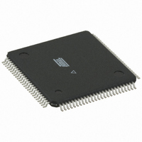
ATMEGA128RZBV-8AU Atmel, ATMEGA128RZBV-8AU Datasheet - Page 374

ATMEGA128RZBV-8AU
Manufacturer Part Number
ATMEGA128RZBV-8AU
Description
MCU ATMEGA1280/AT86RF230 100TQFP
Manufacturer
Atmel
Series
ATMEGAr
Datasheets
1.ATMEGA640V-8CU.pdf
(38 pages)
2.ATMEGA640V-8CU.pdf
(444 pages)
3.AT86RF230-ZU.pdf
(98 pages)
Specifications of ATMEGA128RZBV-8AU
Frequency
2.4GHz
Data Rate - Maximum
2Mbps
Modulation Or Protocol
802.15.4 Zigbee
Applications
General Purpose
Power - Output
3dBm
Sensitivity
-101dBm
Voltage - Supply
1.8 V ~ 3.6 V
Data Interface
PCB, Surface Mount
Memory Size
128kB Flash, 4kB EEPROM, 8kB RAM
Antenna Connector
PCB, Surface Mount
Package / Case
100-TQFP
Wireless Frequency
2.4 GHz
Interface Type
JTAG, SPI
Output Power
3 dBm
For Use With
ATAVRISP2 - PROGRAMMER AVR IN SYSTEMATSTK501 - ADAPTER KIT FOR 64PIN AVR MCUATSTK500 - PROGRAMMER AVR STARTER KIT
Lead Free Status / RoHS Status
Lead free / RoHS Compliant
Operating Temperature
-
Current - Transmitting
-
Current - Receiving
-
Lead Free Status / Rohs Status
Lead free / RoHS Compliant
For Use With/related Products
ATmega128
- Current page: 374 of 444
- Download datasheet (10Mb)
30.7
2549M–AVR–09/10
5. This requirement applies to all ATmega640/1280/1281/2560/2561 2-wire Serial Interface operation. Other devices con-
6. The actual low period generated by the ATmega640/1280/1281/2560/2561 2-wire Serial Interface is (1/f
7. The actual low period generated by the ATmega640/1280/1281/2560/2561 2-wire Serial Interface is (1/f
SPI Timing Characteristics
nected to the 2-wire Serial Bus need only obey the general f
must be greater than 6 MHz for the low time requirement to be strictly met at f
low time requirement will not be strictly met for f
devices connected to the bus may communicate at full speed (400 kHz) with other ATmega640/1280/1281/2560/2561
devices, as well as any other device with a proper t
Figure 30-6. 2-wire Serial Bus Timing
See
Table 30-6.
Note:
SCL
SDA
10
11
12
13
14
15
16
17
18
1
2
3
4
5
6
7
8
9
Figure 30-7 on page 375
t
SU;STA
1. In SPI Programming mode the minimum SCK high/low period is:
- 2 t
- 3 t
SS high to tri-state
SCK to out high
SCK high/low
SCK to SS high
SS low to SCK
SCK high/low
Rise/Fall time
Rise/Fall time
SS low to out
SPI Timing Parameters
Description
CLCL
CLCL
SCK period
SCK period
Out to SCK
SCK to out
SCK to out
Setup
Setup
Hold
Hold
for f
for f
CK
CK
t
HD;STA
< 12 MHz
> 12 MHz
(1)
t
SCL
of
t
LOW
and
LOW
> 308 kHz when f
ATmega640/1280/1281/2560/2561
acceptance margin.
Figure 30-8 on page 375
Master
Master
Master
Master
Master
Master
Master
Master
Mode
t
Slave
Slave
Slave
Slave
Slave
Slave
Slave
Slave
Slave
Slave
HIGH
SCL
t
HD;DAT
requirement.
CK
t
LOW
4 • t
2 • t
= 8 MHz. Still, ATmega640/1280/1281/2560/2561
Min
10
t
20
20
ck
ck
ck
SCL
t
SU;DAT
= 100 kHz.
for details.
See
50% duty cycle
page 203
Table 20-5 on
0.5 • t
Typ
3.6
10
10
10
10
15
15
10
sck
t
SCL
SCL
SU;STO
- 2/f
- 2/f
t
r
1600
Max
CK
CK
), thus the
), thus f
t
BUF
ns
374
CK
Related parts for ATMEGA128RZBV-8AU
Image
Part Number
Description
Manufacturer
Datasheet
Request
R

Part Number:
Description:
Manufacturer:
ATMEL Corporation
Datasheet:

Part Number:
Description:
Microcontroller with 128K bytes In-system programmable flash, 8 MHz, power supply =2.7 - 5.5V
Manufacturer:
ATMEL Corporation
Datasheet:

Part Number:
Description:
IC AVR MCU 128K 16MHZ 5V 64TQFP
Manufacturer:
Atmel
Datasheet:

Part Number:
Description:
IC AVR MCU 128K 16MHZ 5V 64-QFN
Manufacturer:
Atmel
Datasheet:

Part Number:
Description:
IC AVR MCU 128K 16MHZ COM 64-QFN
Manufacturer:
Atmel
Datasheet:

Part Number:
Description:
IC AVR MCU 128K 16MHZ 64-TQFP
Manufacturer:
Atmel
Datasheet:

Part Number:
Description:
IC AVR MCU 128K 16MHZ 64-TQFP
Manufacturer:
Atmel
Datasheet:

Part Number:
Description:
IC AVR MCU 128K 16MHZ IND 64-QFN
Manufacturer:
Atmel
Datasheet:

Part Number:
Description:
MCU AVR 128KB FLASH 16MHZ 64TQFP
Manufacturer:
Atmel
Datasheet:

Part Number:
Description:
MCU AVR 128KB FLASH 16MHZ 64QFN
Manufacturer:
Atmel
Datasheet:

Part Number:
Description:
MCU AVR 128KB FLASH 16MHZ 64TQFP
Manufacturer:
Atmel
Datasheet:


