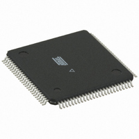
ATMEGA128RZBV-8AU Atmel, ATMEGA128RZBV-8AU Datasheet - Page 281

ATMEGA128RZBV-8AU
Manufacturer Part Number
ATMEGA128RZBV-8AU
Description
MCU ATMEGA1280/AT86RF230 100TQFP
Manufacturer
Atmel
Series
ATMEGAr
Datasheets
1.ATMEGA640V-8CU.pdf
(38 pages)
2.ATMEGA640V-8CU.pdf
(444 pages)
3.AT86RF230-ZU.pdf
(98 pages)
Specifications of ATMEGA128RZBV-8AU
Frequency
2.4GHz
Data Rate - Maximum
2Mbps
Modulation Or Protocol
802.15.4 Zigbee
Applications
General Purpose
Power - Output
3dBm
Sensitivity
-101dBm
Voltage - Supply
1.8 V ~ 3.6 V
Data Interface
PCB, Surface Mount
Memory Size
128kB Flash, 4kB EEPROM, 8kB RAM
Antenna Connector
PCB, Surface Mount
Package / Case
100-TQFP
Wireless Frequency
2.4 GHz
Interface Type
JTAG, SPI
Output Power
3 dBm
For Use With
ATAVRISP2 - PROGRAMMER AVR IN SYSTEMATSTK501 - ADAPTER KIT FOR 64PIN AVR MCUATSTK500 - PROGRAMMER AVR STARTER KIT
Lead Free Status / RoHS Status
Lead free / RoHS Compliant
Operating Temperature
-
Current - Transmitting
-
Current - Receiving
-
Lead Free Status / Rohs Status
Lead free / RoHS Compliant
For Use With/related Products
ATmega128
- Current page: 281 of 444
- Download datasheet (10Mb)
25.4.1
2549M–AVR–09/10
Differential Channels
Table 25-1.
When using differential channels, certain aspects of the conversion need to be taken into
consideration.
Differential conversions are synchronized to the internal clock CK
clock. This synchronization is done automatically by the ADC interface in such a way that the
sample-and-hold occurs at a specific phase of CK
all single conversions, and the first free running conversion) when CK
same amount of time as a single ended conversion (13 ADC clock cycles from the next pres-
caled clock cycle). A conversion initiated by the user when CK
cycles due to the synchronization mechanism. In Free Running mode, a new conversion is initi-
ated immediately after the previous conversion completes, and since CK
all automatically started (that is, all but the first) Free Running conversions will take 14 ADC
clock cycles.
If differential channels are used and conversions are started by Auto Triggering, the ADC must
be switched off between conversions. When Auto Triggering is used, the ADC prescaler is reset
before the conversion is started. Since the stage is dependent of a stable ADC clock prior to the
conversion, this conversion will not be valid. By disabling and then re-enabling the ADC between
each conversion (writing ADEN in ADCSRA to “0” then to “1”), only extended conversions are
performed. The result from the extended conversions will be valid. See
sion Timing” on page 278
Condition
First conversion
Normal conversions, single ended
Auto Triggered conversions
Normal conversions, differential
ADC Conversion Time
for timing details.
ATmega640/1280/1281/2560/2561
Sample & Hold (Cycles from
Start of Conversion)
1.5/2.5
13.5
ADC2
1.5
2
. A conversion initiated by the user (that is,
ADC2
is high will take 14 ADC clock
ADC2
Conversion Time (Cycles)
“Prescaling and Conver-
ADC2
ADC2
equal to half the ADC
is low will take the
is high at this time,
13/14
13.5
25
13
281
Related parts for ATMEGA128RZBV-8AU
Image
Part Number
Description
Manufacturer
Datasheet
Request
R

Part Number:
Description:
Manufacturer:
ATMEL Corporation
Datasheet:

Part Number:
Description:
Microcontroller with 128K bytes In-system programmable flash, 8 MHz, power supply =2.7 - 5.5V
Manufacturer:
ATMEL Corporation
Datasheet:

Part Number:
Description:
IC AVR MCU 128K 16MHZ 5V 64TQFP
Manufacturer:
Atmel
Datasheet:

Part Number:
Description:
IC AVR MCU 128K 16MHZ 5V 64-QFN
Manufacturer:
Atmel
Datasheet:

Part Number:
Description:
IC AVR MCU 128K 16MHZ COM 64-QFN
Manufacturer:
Atmel
Datasheet:

Part Number:
Description:
IC AVR MCU 128K 16MHZ 64-TQFP
Manufacturer:
Atmel
Datasheet:

Part Number:
Description:
IC AVR MCU 128K 16MHZ 64-TQFP
Manufacturer:
Atmel
Datasheet:

Part Number:
Description:
IC AVR MCU 128K 16MHZ IND 64-QFN
Manufacturer:
Atmel
Datasheet:

Part Number:
Description:
MCU AVR 128KB FLASH 16MHZ 64TQFP
Manufacturer:
Atmel
Datasheet:

Part Number:
Description:
MCU AVR 128KB FLASH 16MHZ 64QFN
Manufacturer:
Atmel
Datasheet:

Part Number:
Description:
MCU AVR 128KB FLASH 16MHZ 64TQFP
Manufacturer:
Atmel
Datasheet:


