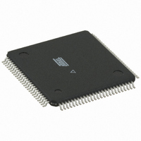
ATMEGA128RZBV-8AU Atmel, ATMEGA128RZBV-8AU Datasheet - Page 295

ATMEGA128RZBV-8AU
Manufacturer Part Number
ATMEGA128RZBV-8AU
Description
MCU ATMEGA1280/AT86RF230 100TQFP
Manufacturer
Atmel
Series
ATMEGAr
Datasheets
1.ATMEGA640V-8CU.pdf
(38 pages)
2.ATMEGA640V-8CU.pdf
(444 pages)
3.AT86RF230-ZU.pdf
(98 pages)
Specifications of ATMEGA128RZBV-8AU
Frequency
2.4GHz
Data Rate - Maximum
2Mbps
Modulation Or Protocol
802.15.4 Zigbee
Applications
General Purpose
Power - Output
3dBm
Sensitivity
-101dBm
Voltage - Supply
1.8 V ~ 3.6 V
Data Interface
PCB, Surface Mount
Memory Size
128kB Flash, 4kB EEPROM, 8kB RAM
Antenna Connector
PCB, Surface Mount
Package / Case
100-TQFP
Wireless Frequency
2.4 GHz
Interface Type
JTAG, SPI
Output Power
3 dBm
For Use With
ATAVRISP2 - PROGRAMMER AVR IN SYSTEMATSTK501 - ADAPTER KIT FOR 64PIN AVR MCUATSTK500 - PROGRAMMER AVR STARTER KIT
Lead Free Status / RoHS Status
Lead free / RoHS Compliant
Operating Temperature
-
Current - Transmitting
-
Current - Receiving
-
Lead Free Status / Rohs Status
Lead free / RoHS Compliant
For Use With/related Products
ATmega128
- Current page: 295 of 444
- Download datasheet (10Mb)
25.8.6
25.8.7
2549M–AVR–09/10
DIDR0 – Digital Input Disable Register 0
DIDR2 – Digital Input Disable Register 2
ger source that is cleared to a trigger source that is set, will generate a positive edge on the
trigger signal. If ADEN in ADCSRA is set, this will start a conversion. Switching to Free Running
mode (ADTS[2:0]=0) will not cause a trigger event, even if the ADC Interrupt Flag is set
Table 25-6.
Note:
• Bit 7:0 – ADC7D:ADC0D: ADC7:0 Digital Input Disable
When this bit is written logic one, the digital input buffer on the corresponding ADC pin is dis-
abled. The corresponding PIN Register bit will always read as zero when this bit is set. When an
analog signal is applied to the ADC7:0 pin and the digital input from this pin is not needed, this
bit should be written logic one to reduce power consumption in the digital input buffer.
• Bit 7:0 – ADC15D:ADC8D: ADC15:8 Digital Input Disable
When this bit is written logic one, the digital input buffer on the corresponding ADC pin is dis-
abled. The corresponding PIN Register bit will always read as zero when this bit is set. When an
analog signal is applied to the ADC15:8 pin and the digital input from this pin is not needed, this
bit should be written logic one to reduce power consumption in the digital input buffer.
Bit
(0x7E)
Read/Write
Initial Value
Bit
(0x7D)
Read/Write
Initial Value
ADTS2
Free running mode cannot be used for differential channels (see chapter
on page
0
0
0
0
1
1
1
1
ADC15D
ADC7D
ADC Auto Trigger Source Selections
R/W
R/W
7
0
7
0
281).
ADC14D
ADC6D
R/W
R/W
ADTS1
6
0
6
0
0
0
1
1
0
0
1
1
ADC13D
ATmega640/1280/1281/2560/2561
ADC5D
R/W
R/W
5
0
5
0
ADC12D
ADC4D
R/W
R/W
ADTS0
4
0
4
0
0
1
0
1
0
1
0
1
ADC11D
ADC3D
R/W
R/W
3
0
3
0
Trigger Source
Free Running mode
Analog Comparator
External Interrupt Request 0
Timer/Counter0 Compare Match A
Timer/Counter0 Overflow
Timer/Counter1 Compare Match B
Timer/Counter1 Overflow
Timer/Counter1 Capture Event
ADC10D
ADC2D
R/W
R/W
2
0
2
0
ADC1D
ADC9D
R/W
R/W
1
0
1
0
“Differential Channels”
ADC0D
ADC8D
R/W
R/W
0
0
0
0
.
DIDR0
DIDR2
295
Related parts for ATMEGA128RZBV-8AU
Image
Part Number
Description
Manufacturer
Datasheet
Request
R

Part Number:
Description:
Manufacturer:
ATMEL Corporation
Datasheet:

Part Number:
Description:
Microcontroller with 128K bytes In-system programmable flash, 8 MHz, power supply =2.7 - 5.5V
Manufacturer:
ATMEL Corporation
Datasheet:

Part Number:
Description:
IC AVR MCU 128K 16MHZ 5V 64TQFP
Manufacturer:
Atmel
Datasheet:

Part Number:
Description:
IC AVR MCU 128K 16MHZ 5V 64-QFN
Manufacturer:
Atmel
Datasheet:

Part Number:
Description:
IC AVR MCU 128K 16MHZ COM 64-QFN
Manufacturer:
Atmel
Datasheet:

Part Number:
Description:
IC AVR MCU 128K 16MHZ 64-TQFP
Manufacturer:
Atmel
Datasheet:

Part Number:
Description:
IC AVR MCU 128K 16MHZ 64-TQFP
Manufacturer:
Atmel
Datasheet:

Part Number:
Description:
IC AVR MCU 128K 16MHZ IND 64-QFN
Manufacturer:
Atmel
Datasheet:

Part Number:
Description:
MCU AVR 128KB FLASH 16MHZ 64TQFP
Manufacturer:
Atmel
Datasheet:

Part Number:
Description:
MCU AVR 128KB FLASH 16MHZ 64QFN
Manufacturer:
Atmel
Datasheet:

Part Number:
Description:
MCU AVR 128KB FLASH 16MHZ 64TQFP
Manufacturer:
Atmel
Datasheet:


