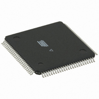
ATMEGA128RZBV-8AU Atmel, ATMEGA128RZBV-8AU Datasheet - Page 32

ATMEGA128RZBV-8AU
Manufacturer Part Number
ATMEGA128RZBV-8AU
Description
MCU ATMEGA1280/AT86RF230 100TQFP
Manufacturer
Atmel
Series
ATMEGAr
Datasheets
1.ATMEGA640V-8CU.pdf
(38 pages)
2.ATMEGA640V-8CU.pdf
(444 pages)
3.AT86RF230-ZU.pdf
(98 pages)
Specifications of ATMEGA128RZBV-8AU
Frequency
2.4GHz
Data Rate - Maximum
2Mbps
Modulation Or Protocol
802.15.4 Zigbee
Applications
General Purpose
Power - Output
3dBm
Sensitivity
-101dBm
Voltage - Supply
1.8 V ~ 3.6 V
Data Interface
PCB, Surface Mount
Memory Size
128kB Flash, 4kB EEPROM, 8kB RAM
Antenna Connector
PCB, Surface Mount
Package / Case
100-TQFP
Wireless Frequency
2.4 GHz
Interface Type
JTAG, SPI
Output Power
3 dBm
For Use With
ATAVRISP2 - PROGRAMMER AVR IN SYSTEMATSTK501 - ADAPTER KIT FOR 64PIN AVR MCUATSTK500 - PROGRAMMER AVR STARTER KIT
Lead Free Status / RoHS Status
Lead free / RoHS Compliant
Operating Temperature
-
Current - Transmitting
-
Current - Receiving
-
Lead Free Status / Rohs Status
Lead free / RoHS Compliant
For Use With/related Products
ATmega128
- Current page: 32 of 444
- Download datasheet (10Mb)
8.1.5
2549M–AVR–09/10
Using all Locations of External Memory Smaller than 64 Kbytes
Figure 8-5.
Note:
Figure 8-6.
Note:
Since the external memory is mapped after the internal memory as shown in
28, the external memory is not addressed when addressing the first 8,704 bytes of data space. It
may appear that the first 8,704 bytes of the external memory are inaccessible (external memory
addresses 0x0000 to 0x21FF). However, when connecting an external memory smaller than 64
Kbytes, for example 32 Kbytes, these locations are easily accessed simply by addressing from
address 0x8000 to 0xA1FF. Since the External Memory Address bit A15 is not connected to the
external memory, addresses 0x8000 to 0xA1FF will appear as addresses 0x0000 to 0x21FF for
the external memory. Addressing above address 0xA1FF is not recommended, since this will
address an external memory location that is already accessed by another (lower) address. To
System Clock (CLK
System Clock (CLK
DA7:0 (XMBK = 0)
DA7:0 (XMBK = 1)
DA7:0 (XMBK = 0)
DA7:0 (XMBK = 1)
1. SRWn1 = SRW11 (upper sector) or SRW01 (lower sector), SRWn0 = SRW10 (upper sector) or
1. SRWn1 = SRW11 (upper sector) or SRW01 (lower sector), SRWn0 = SRW10 (upper sector) or
SRW00 (lower sector).
The ALE pulse in period T6 is only present if the next instruction accesses the RAM (internal
or external).
SRW00 (lower sector).
The ALE pulse in period T7 is only present if the next instruction accesses the RAM (internal
or external).
DA7:0
A15:8
CPU
ALE
DA7:0
WR
A15:8
RD
External Data Memory Cycles with SRWn1 = 1 and SRWn0 = 0
External Data Memory Cycles with SRWn1 = 1 and SRWn0 = 1
CPU
ALE
WR
)
RD
)
Prev. addr.
Prev. data
Prev. data
Prev. data
Prev. addr.
Prev. data
Prev. data
Prev. data
T1
T1
Address
Address
Address
ATmega640/1280/1281/2560/2561
T2
Address
Address
Address
XX
T2
XX
Address
T3
Data
Data
Data
Address
T3
Data
Data
Data
T4
T4
T5
T5
T6
Figure 8-1 on page
(1)
(1)
T6
T7
32
Related parts for ATMEGA128RZBV-8AU
Image
Part Number
Description
Manufacturer
Datasheet
Request
R

Part Number:
Description:
Manufacturer:
ATMEL Corporation
Datasheet:

Part Number:
Description:
Microcontroller with 128K bytes In-system programmable flash, 8 MHz, power supply =2.7 - 5.5V
Manufacturer:
ATMEL Corporation
Datasheet:

Part Number:
Description:
IC AVR MCU 128K 16MHZ 5V 64TQFP
Manufacturer:
Atmel
Datasheet:

Part Number:
Description:
IC AVR MCU 128K 16MHZ 5V 64-QFN
Manufacturer:
Atmel
Datasheet:

Part Number:
Description:
IC AVR MCU 128K 16MHZ COM 64-QFN
Manufacturer:
Atmel
Datasheet:

Part Number:
Description:
IC AVR MCU 128K 16MHZ 64-TQFP
Manufacturer:
Atmel
Datasheet:

Part Number:
Description:
IC AVR MCU 128K 16MHZ 64-TQFP
Manufacturer:
Atmel
Datasheet:

Part Number:
Description:
IC AVR MCU 128K 16MHZ IND 64-QFN
Manufacturer:
Atmel
Datasheet:

Part Number:
Description:
MCU AVR 128KB FLASH 16MHZ 64TQFP
Manufacturer:
Atmel
Datasheet:

Part Number:
Description:
MCU AVR 128KB FLASH 16MHZ 64QFN
Manufacturer:
Atmel
Datasheet:

Part Number:
Description:
MCU AVR 128KB FLASH 16MHZ 64TQFP
Manufacturer:
Atmel
Datasheet:


