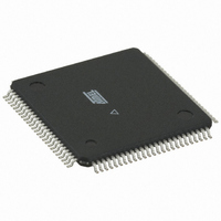
ATMEGA128RZBV-8AU Atmel, ATMEGA128RZBV-8AU Datasheet - Page 115

ATMEGA128RZBV-8AU
Manufacturer Part Number
ATMEGA128RZBV-8AU
Description
MCU ATMEGA1280/AT86RF230 100TQFP
Manufacturer
Atmel
Series
ATMEGAr
Datasheets
1.ATMEGA640V-8CU.pdf
(38 pages)
2.ATMEGA640V-8CU.pdf
(444 pages)
3.AT86RF230-ZU.pdf
(98 pages)
Specifications of ATMEGA128RZBV-8AU
Frequency
2.4GHz
Data Rate - Maximum
2Mbps
Modulation Or Protocol
802.15.4 Zigbee
Applications
General Purpose
Power - Output
3dBm
Sensitivity
-101dBm
Voltage - Supply
1.8 V ~ 3.6 V
Data Interface
PCB, Surface Mount
Memory Size
128kB Flash, 4kB EEPROM, 8kB RAM
Antenna Connector
PCB, Surface Mount
Package / Case
100-TQFP
Wireless Frequency
2.4 GHz
Interface Type
JTAG, SPI
Output Power
3 dBm
For Use With
ATAVRISP2 - PROGRAMMER AVR IN SYSTEMATSTK501 - ADAPTER KIT FOR 64PIN AVR MCUATSTK500 - PROGRAMMER AVR STARTER KIT
Lead Free Status / RoHS Status
Lead free / RoHS Compliant
Operating Temperature
-
Current - Transmitting
-
Current - Receiving
-
Lead Free Status / Rohs Status
Lead free / RoHS Compliant
For Use With/related Products
ATmega128
- Current page: 115 of 444
- Download datasheet (10Mb)
14.2.3
14.2.4
14.2.5
2549M–AVR–09/10
EIMSK – External Interrupt Mask Register
EIFR – External Interrupt Flag Register
PCICR – Pin Change Interrupt Control Register
• Bits 7:0 – INT7:0: External Interrupt Request 7 - 0 Enable
When an INT7:0 bit is written to one and the I-bit in the Status Register (SREG) is set (one), the
corresponding external pin interrupt is enabled. The Interrupt Sense Control bits in the External
Interrupt Control Registers – EICRA and EICRB – defines whether the external interrupt is acti-
vated on rising or falling edge or level sensed. Activity on any of these pins will trigger an
interrupt request even if the pin is enabled as an output. This provides a way of generating a
software interrupt.
• Bits 7:0 – INTF7:0: External Interrupt Flags 7 - 0
When an edge or logic change on the INT7:0 pin triggers an interrupt request, INTF7:0 becomes
set (one). If the I-bit in SREG and the corresponding interrupt enable bit, INT7:0 in EIMSK, are
set (one), the MCU will jump to the interrupt vector. The flag is cleared when the interrupt routine
is executed. Alternatively, the flag can be cleared by writing a logical one to it. These flags are
always cleared when INT7:0 are configured as level interrupt. Note that when entering sleep
mode with the INT3:0 interrupts disabled, the input buffers on these pins will be disabled. This
may cause a logic change in internal signals which will set the INTF3:0 flags. See
Enable and Sleep Modes” on page 74
• Bit 2 – PCIE2: Pin Change Interrupt Enable 1
When the PCIE2 bit is set (one) and the I-bit in the Status Register (SREG) is set (one), pin
change interrupt 2 is enabled. Any change on any enabled PCINT23:16 pin will cause an inter-
rupt. The corresponding interrupt of Pin Change Interrupt Request is executed from the PCI2
Interrupt Vector. PCINT23:16 pins are enabled individually by the PCMSK2 Register.
• Bit 1 – PCIE1: Pin Change Interrupt Enable 1
When the PCIE1 bit is set (one) and the I-bit in the Status Register (SREG) is set (one), pin
change interrupt 1 is enabled. Any change on any enabled PCINT15:8 pin will cause an inter-
rupt. The corresponding interrupt of Pin Change Interrupt Request is executed from the PCI1
Interrupt Vector. PCINT15:8 pins are enabled individually by the PCMSK1 Register.
Bit
0x1D (0x3D)
Read/Write
Initial Value
Bit
0x1C (0x3C)
Read/Write
Initial Value
Bit
(0x68)
Read/Write
Initial Value
INTF7
INT7
R/W
R/W
7
0
7
0
R
7
–
0
INTF6
INT6
R/W
R/W
6
0
6
0
R
6
–
0
ATmega640/1280/1281/2560/2561
INTF5
INT5
R/W
R/W
5
0
5
0
R
5
–
0
for more information.
INTF4
INT4
R/W
R/W
4
0
4
0
R
4
–
0
INTF3
INT3
R/W
R/W
3
0
3
0
R
3
–
0
INTF2
INT2
PCIE2
R/W
R/W
R/W
2
0
2
0
2
0
INTF1
INT1
PCIE1
R/W
R/W
R/W
1
0
1
0
1
0
IINTF0
INT0
R/W
R/W
PCIE0
R/W
0
0
0
0
0
0
“Digital Input
EIMSK
PCICR
EIFR
115
Related parts for ATMEGA128RZBV-8AU
Image
Part Number
Description
Manufacturer
Datasheet
Request
R

Part Number:
Description:
Manufacturer:
ATMEL Corporation
Datasheet:

Part Number:
Description:
Microcontroller with 128K bytes In-system programmable flash, 8 MHz, power supply =2.7 - 5.5V
Manufacturer:
ATMEL Corporation
Datasheet:

Part Number:
Description:
IC AVR MCU 128K 16MHZ 5V 64TQFP
Manufacturer:
Atmel
Datasheet:

Part Number:
Description:
IC AVR MCU 128K 16MHZ 5V 64-QFN
Manufacturer:
Atmel
Datasheet:

Part Number:
Description:
IC AVR MCU 128K 16MHZ COM 64-QFN
Manufacturer:
Atmel
Datasheet:

Part Number:
Description:
IC AVR MCU 128K 16MHZ 64-TQFP
Manufacturer:
Atmel
Datasheet:

Part Number:
Description:
IC AVR MCU 128K 16MHZ 64-TQFP
Manufacturer:
Atmel
Datasheet:

Part Number:
Description:
IC AVR MCU 128K 16MHZ IND 64-QFN
Manufacturer:
Atmel
Datasheet:

Part Number:
Description:
MCU AVR 128KB FLASH 16MHZ 64TQFP
Manufacturer:
Atmel
Datasheet:

Part Number:
Description:
MCU AVR 128KB FLASH 16MHZ 64QFN
Manufacturer:
Atmel
Datasheet:

Part Number:
Description:
MCU AVR 128KB FLASH 16MHZ 64TQFP
Manufacturer:
Atmel
Datasheet:


