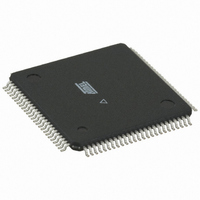
ATMEGA128RZBV-8AU Atmel, ATMEGA128RZBV-8AU Datasheet - Page 243

ATMEGA128RZBV-8AU
Manufacturer Part Number
ATMEGA128RZBV-8AU
Description
MCU ATMEGA1280/AT86RF230 100TQFP
Manufacturer
Atmel
Series
ATMEGAr
Datasheets
1.ATMEGA640V-8CU.pdf
(38 pages)
2.ATMEGA640V-8CU.pdf
(444 pages)
3.AT86RF230-ZU.pdf
(98 pages)
Specifications of ATMEGA128RZBV-8AU
Frequency
2.4GHz
Data Rate - Maximum
2Mbps
Modulation Or Protocol
802.15.4 Zigbee
Applications
General Purpose
Power - Output
3dBm
Sensitivity
-101dBm
Voltage - Supply
1.8 V ~ 3.6 V
Data Interface
PCB, Surface Mount
Memory Size
128kB Flash, 4kB EEPROM, 8kB RAM
Antenna Connector
PCB, Surface Mount
Package / Case
100-TQFP
Wireless Frequency
2.4 GHz
Interface Type
JTAG, SPI
Output Power
3 dBm
For Use With
ATAVRISP2 - PROGRAMMER AVR IN SYSTEMATSTK501 - ADAPTER KIT FOR 64PIN AVR MCUATSTK500 - PROGRAMMER AVR STARTER KIT
Lead Free Status / RoHS Status
Lead free / RoHS Compliant
Operating Temperature
-
Current - Transmitting
-
Current - Receiving
-
Lead Free Status / Rohs Status
Lead free / RoHS Compliant
For Use With/related Products
ATmega128
- Current page: 243 of 444
- Download datasheet (10Mb)
23.3.3
2549M–AVR–09/10
Address Packet Format
Figure 23-3. START, REPEATED START and STOP conditions
All address packets transmitted on the TWI bus are 9 bits long, consisting of 7 address bits, one
READ/WRITE control bit and an acknowledge bit. If the READ/WRITE bit is set, a read opera-
tion is to be performed, otherwise a write operation should be performed. When a Slave
recognizes that it is being addressed, it should acknowledge by pulling SDA low in the ninth SCL
(ACK) cycle. If the addressed Slave is busy, or for some other reason can not service the Mas-
ter’s request, the SDA line should be left high in the ACK clock cycle. The Master can then
transmit a STOP condition, or a REPEATED START condition to initiate a new transmission. An
address packet consisting of a slave address and a READ or a WRITE bit is called SLA+R or
SLA+W, respectively.
The MSB of the address byte is transmitted first. Slave addresses can freely be allocated by the
designer, but the address 0000 000 is reserved for a general call.
When a general call is issued, all slaves should respond by pulling the SDA line low in the ACK
cycle. A general call is used when a Master wishes to transmit the same message to several
slaves in the system. When the general call address followed by a Write bit is transmitted on the
bus, all slaves set up to acknowledge the general call will pull the SDA line low in the ack cycle.
The following data packets will then be received by all the slaves that acknowledged the general
call. Note that transmitting the general call address followed by a Read bit is meaningless, as
this would cause contention if several slaves started transmitting different data.
All addresses of the format 1111 xxx should be reserved for future purposes.
Figure 23-4. Address Packet Format
SDA
SCL
SDA
SCL
START
START
Addr MSB
1
ATmega640/1280/1281/2560/2561
STOP
2
START
Addr LSB
7
REPEATED START
R/W
8
ACK
9
STOP
243
Related parts for ATMEGA128RZBV-8AU
Image
Part Number
Description
Manufacturer
Datasheet
Request
R

Part Number:
Description:
Manufacturer:
ATMEL Corporation
Datasheet:

Part Number:
Description:
Microcontroller with 128K bytes In-system programmable flash, 8 MHz, power supply =2.7 - 5.5V
Manufacturer:
ATMEL Corporation
Datasheet:

Part Number:
Description:
IC AVR MCU 128K 16MHZ 5V 64TQFP
Manufacturer:
Atmel
Datasheet:

Part Number:
Description:
IC AVR MCU 128K 16MHZ 5V 64-QFN
Manufacturer:
Atmel
Datasheet:

Part Number:
Description:
IC AVR MCU 128K 16MHZ COM 64-QFN
Manufacturer:
Atmel
Datasheet:

Part Number:
Description:
IC AVR MCU 128K 16MHZ 64-TQFP
Manufacturer:
Atmel
Datasheet:

Part Number:
Description:
IC AVR MCU 128K 16MHZ 64-TQFP
Manufacturer:
Atmel
Datasheet:

Part Number:
Description:
IC AVR MCU 128K 16MHZ IND 64-QFN
Manufacturer:
Atmel
Datasheet:

Part Number:
Description:
MCU AVR 128KB FLASH 16MHZ 64TQFP
Manufacturer:
Atmel
Datasheet:

Part Number:
Description:
MCU AVR 128KB FLASH 16MHZ 64QFN
Manufacturer:
Atmel
Datasheet:

Part Number:
Description:
MCU AVR 128KB FLASH 16MHZ 64TQFP
Manufacturer:
Atmel
Datasheet:


