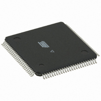
ATMEGA128RZBV-8AU Atmel, ATMEGA128RZBV-8AU Datasheet - Page 202

ATMEGA128RZBV-8AU
Manufacturer Part Number
ATMEGA128RZBV-8AU
Description
MCU ATMEGA1280/AT86RF230 100TQFP
Manufacturer
Atmel
Series
ATMEGAr
Datasheets
1.ATMEGA640V-8CU.pdf
(38 pages)
2.ATMEGA640V-8CU.pdf
(444 pages)
3.AT86RF230-ZU.pdf
(98 pages)
Specifications of ATMEGA128RZBV-8AU
Frequency
2.4GHz
Data Rate - Maximum
2Mbps
Modulation Or Protocol
802.15.4 Zigbee
Applications
General Purpose
Power - Output
3dBm
Sensitivity
-101dBm
Voltage - Supply
1.8 V ~ 3.6 V
Data Interface
PCB, Surface Mount
Memory Size
128kB Flash, 4kB EEPROM, 8kB RAM
Antenna Connector
PCB, Surface Mount
Package / Case
100-TQFP
Wireless Frequency
2.4 GHz
Interface Type
JTAG, SPI
Output Power
3 dBm
For Use With
ATAVRISP2 - PROGRAMMER AVR IN SYSTEMATSTK501 - ADAPTER KIT FOR 64PIN AVR MCUATSTK500 - PROGRAMMER AVR STARTER KIT
Lead Free Status / RoHS Status
Lead free / RoHS Compliant
Operating Temperature
-
Current - Transmitting
-
Current - Receiving
-
Lead Free Status / Rohs Status
Lead free / RoHS Compliant
For Use With/related Products
ATmega128
- Current page: 202 of 444
- Download datasheet (10Mb)
20.2
20.2.1
2549M–AVR–09/10
Register Description
SPCR – SPI Control Register
• Bit 7 – SPIE: SPI Interrupt Enable
This bit causes the SPI interrupt to be executed if SPIF bit in the SPSR Register is set and the if
the Global Interrupt Enable bit in SREG is set.
• Bit 6 – SPE: SPI Enable
When the SPE bit is written to one, the SPI is enabled. This bit must be set to enable any SPI
operations.
• Bit 5 – DORD: Data Order
When the DORD bit is written to one, the LSB of the data word is transmitted first.
When the DORD bit is written to zero, the MSB of the data word is transmitted first.
• Bit 4 – MSTR: Master/Slave Select
This bit selects Master SPI mode when written to one, and Slave SPI mode when written logic
zero. If SS is configured as an input and is driven low while MSTR is set, MSTR will be cleared,
and SPIF in SPSR will become set. The user will then have to set MSTR to re-enable SPI Mas-
ter mode.
• Bit 3 – CPOL: Clock Polarity
When this bit is written to one, SCK is high when idle. When CPOL is written to zero, SCK is low
when idle. Refer to
CPOL functionality is summarized in
Table 20-3.
• Bit 2 – CPHA: Clock Phase
The settings of the Clock Phase bit (CPHA) determine if data is sampled on the leading (first) or
trailing (last) edge of SCK. Refer to
example. The CPOL functionality is summarized in
Table 20-4.
Bit
0x2C (0x4C)
Read/Write
Initial Value
CPOL
CPHA
CPOL Functionality
CPHA Functionality
0
1
0
1
SPIE
R/W
7
0
Figure 20-3 on page 201
SPE
R/W
6
0
ATmega640/1280/1281/2560/2561
DORD
R/W
Figure 20-3 on page 201
5
0
Table
Leading Edge
Leading Edge
MSTR
Sample
Falling
20-3.
Rising
R/W
Setup
4
0
and
Figure 20-4 on page 201
Table
CPOL
R/W
3
0
20-4.
and
CPHA
R/W
2
0
Figure 20-4 on page 201
SPR1
R/W
1
0
Trailing Edge
Trailing Edge
Sample
for an example. The
Falling
Rising
Setup
SPR0
R/W
0
0
SPCR
for an
202
Related parts for ATMEGA128RZBV-8AU
Image
Part Number
Description
Manufacturer
Datasheet
Request
R

Part Number:
Description:
Manufacturer:
ATMEL Corporation
Datasheet:

Part Number:
Description:
Microcontroller with 128K bytes In-system programmable flash, 8 MHz, power supply =2.7 - 5.5V
Manufacturer:
ATMEL Corporation
Datasheet:

Part Number:
Description:
IC AVR MCU 128K 16MHZ 5V 64TQFP
Manufacturer:
Atmel
Datasheet:

Part Number:
Description:
IC AVR MCU 128K 16MHZ 5V 64-QFN
Manufacturer:
Atmel
Datasheet:

Part Number:
Description:
IC AVR MCU 128K 16MHZ COM 64-QFN
Manufacturer:
Atmel
Datasheet:

Part Number:
Description:
IC AVR MCU 128K 16MHZ 64-TQFP
Manufacturer:
Atmel
Datasheet:

Part Number:
Description:
IC AVR MCU 128K 16MHZ 64-TQFP
Manufacturer:
Atmel
Datasheet:

Part Number:
Description:
IC AVR MCU 128K 16MHZ IND 64-QFN
Manufacturer:
Atmel
Datasheet:

Part Number:
Description:
MCU AVR 128KB FLASH 16MHZ 64TQFP
Manufacturer:
Atmel
Datasheet:

Part Number:
Description:
MCU AVR 128KB FLASH 16MHZ 64QFN
Manufacturer:
Atmel
Datasheet:

Part Number:
Description:
MCU AVR 128KB FLASH 16MHZ 64TQFP
Manufacturer:
Atmel
Datasheet:


