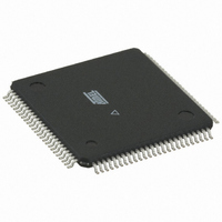
ATMEGA128RZBV-8AU Atmel, ATMEGA128RZBV-8AU Datasheet - Page 337

ATMEGA128RZBV-8AU
Manufacturer Part Number
ATMEGA128RZBV-8AU
Description
MCU ATMEGA1280/AT86RF230 100TQFP
Manufacturer
Atmel
Series
ATMEGAr
Datasheets
1.ATMEGA640V-8CU.pdf
(38 pages)
2.ATMEGA640V-8CU.pdf
(444 pages)
3.AT86RF230-ZU.pdf
(98 pages)
Specifications of ATMEGA128RZBV-8AU
Frequency
2.4GHz
Data Rate - Maximum
2Mbps
Modulation Or Protocol
802.15.4 Zigbee
Applications
General Purpose
Power - Output
3dBm
Sensitivity
-101dBm
Voltage - Supply
1.8 V ~ 3.6 V
Data Interface
PCB, Surface Mount
Memory Size
128kB Flash, 4kB EEPROM, 8kB RAM
Antenna Connector
PCB, Surface Mount
Package / Case
100-TQFP
Wireless Frequency
2.4 GHz
Interface Type
JTAG, SPI
Output Power
3 dBm
For Use With
ATAVRISP2 - PROGRAMMER AVR IN SYSTEMATSTK501 - ADAPTER KIT FOR 64PIN AVR MCUATSTK500 - PROGRAMMER AVR STARTER KIT
Lead Free Status / RoHS Status
Lead free / RoHS Compliant
Operating Temperature
-
Current - Transmitting
-
Current - Receiving
-
Lead Free Status / Rohs Status
Lead free / RoHS Compliant
For Use With/related Products
ATmega128
- Current page: 337 of 444
- Download datasheet (10Mb)
2549M–AVR–09/10
Table 29-4.
Notes:
Table 29-5.
Notes:
The status of the Fuse bits is not affected by Chip Erase. Note that the Fuse bits are locked if
Lock bit1 (LB1) is programmed. Program the Fuse bits before programming the Lock bits.
Fuse High Byte
OCDEN
JTAGEN
SPIEN
WDTON
EESAVE
BOOTSZ1
BOOTSZ0
BOOTRST
Fuse Low Byte
CKDIV8
CKOUT
SUT1
SUT0
CKSEL3
CKSEL2
CKSEL1
CKSEL0
(1)
1. The SPIEN Fuse is not accessible in serial programming mode.
2. The default value of BOOTSZ1:0 results in maximum Boot Size. See
3. See
4. Never ship a product with the OCDEN Fuse programmed regardless of the setting of Lock bits
1. The default value of SUT1:0 results in maximum start-up time for the default clock source. See
2. The default setting of CKSEL3:0 results in internal RC Oscillator @ 8 MHz. See
3. The CKOUT Fuse allow the system clock to be output on PORTE7. See
4. See
(3)
(4)
(4)
(3)
for details.
and JTAGEN Fuse. A programmed OCDEN Fuse enables some parts of the clock system to
be running in all sleep modes. This may increase the power consumption.
“System and Reset Characteristics” on page 372
page 41
on page 49
Fuse High Byte
Fuse Low Byte
“WDTCSR – Watchdog Timer Control Register” on page 67
“System Clock Prescaler” on page 49
for details.
Bit No
for details.
7
6
5
4
3
2
1
0
Bit No
7
6
5
4
3
2
1
0
Description
Enable OCD
Enable JTAG
Enable Serial Program and Data
Downloading
Watchdog Timer always on
EEPROM memory is preserved
through the Chip Erase
Select Boot Size (see
page 339
Select Boot Size (see
page 339
Select Reset Vector
ATmega640/1280/1281/2560/2561
Description
Divide clock by 8
Clock output
Select start-up time
Select start-up time
Select Clock source
Select Clock source
Select Clock source
Select Clock source
for details)
for details)
for details.
Table 29-9 on
Table 29-9 on
for details.
Default Value
1 (unprogrammed, OCD
disabled)
0 (programmed, JTAG enabled)
0 (programmed, SPI prog.
enabled)
1 (unprogrammed)
1 (unprogrammed, EEPROM
not preserved)
0 (programmed)
0 (programmed)
1 (unprogrammed)
1 (unprogrammed)
Default Value
0 (programmed)
1 (unprogrammed)
0 (programmed)
0 (programmed)
0 (programmed)
1 (unprogrammed)
0 (programmed)
for details.
Table 28-7 on page 328
“Clock Output Buffer”
(2)
(2)
(1)
(2)
(2)
(2)
Table 9-1 on
(1)
(2)
337
Related parts for ATMEGA128RZBV-8AU
Image
Part Number
Description
Manufacturer
Datasheet
Request
R

Part Number:
Description:
Manufacturer:
ATMEL Corporation
Datasheet:

Part Number:
Description:
Microcontroller with 128K bytes In-system programmable flash, 8 MHz, power supply =2.7 - 5.5V
Manufacturer:
ATMEL Corporation
Datasheet:

Part Number:
Description:
IC AVR MCU 128K 16MHZ 5V 64TQFP
Manufacturer:
Atmel
Datasheet:

Part Number:
Description:
IC AVR MCU 128K 16MHZ 5V 64-QFN
Manufacturer:
Atmel
Datasheet:

Part Number:
Description:
IC AVR MCU 128K 16MHZ COM 64-QFN
Manufacturer:
Atmel
Datasheet:

Part Number:
Description:
IC AVR MCU 128K 16MHZ 64-TQFP
Manufacturer:
Atmel
Datasheet:

Part Number:
Description:
IC AVR MCU 128K 16MHZ 64-TQFP
Manufacturer:
Atmel
Datasheet:

Part Number:
Description:
IC AVR MCU 128K 16MHZ IND 64-QFN
Manufacturer:
Atmel
Datasheet:

Part Number:
Description:
MCU AVR 128KB FLASH 16MHZ 64TQFP
Manufacturer:
Atmel
Datasheet:

Part Number:
Description:
MCU AVR 128KB FLASH 16MHZ 64QFN
Manufacturer:
Atmel
Datasheet:

Part Number:
Description:
MCU AVR 128KB FLASH 16MHZ 64TQFP
Manufacturer:
Atmel
Datasheet:


