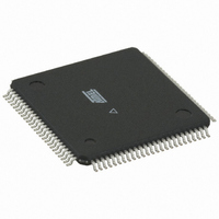
ATMEGA128RZBV-8AU Atmel, ATMEGA128RZBV-8AU Datasheet - Page 304

ATMEGA128RZBV-8AU
Manufacturer Part Number
ATMEGA128RZBV-8AU
Description
MCU ATMEGA1280/AT86RF230 100TQFP
Manufacturer
Atmel
Series
ATMEGAr
Datasheets
1.ATMEGA640V-8CU.pdf
(38 pages)
2.ATMEGA640V-8CU.pdf
(444 pages)
3.AT86RF230-ZU.pdf
(98 pages)
Specifications of ATMEGA128RZBV-8AU
Frequency
2.4GHz
Data Rate - Maximum
2Mbps
Modulation Or Protocol
802.15.4 Zigbee
Applications
General Purpose
Power - Output
3dBm
Sensitivity
-101dBm
Voltage - Supply
1.8 V ~ 3.6 V
Data Interface
PCB, Surface Mount
Memory Size
128kB Flash, 4kB EEPROM, 8kB RAM
Antenna Connector
PCB, Surface Mount
Package / Case
100-TQFP
Wireless Frequency
2.4 GHz
Interface Type
JTAG, SPI
Output Power
3 dBm
For Use With
ATAVRISP2 - PROGRAMMER AVR IN SYSTEMATSTK501 - ADAPTER KIT FOR 64PIN AVR MCUATSTK500 - PROGRAMMER AVR STARTER KIT
Lead Free Status / RoHS Status
Lead free / RoHS Compliant
Operating Temperature
-
Current - Transmitting
-
Current - Receiving
-
Lead Free Status / Rohs Status
Lead free / RoHS Compliant
For Use With/related Products
ATmega128
- Current page: 304 of 444
- Download datasheet (10Mb)
27.3.4
27.4
27.4.1
27.4.2
2549M–AVR–09/10
Boundary-scan Specific JTAG Instructions
Boundary-scan Chain
EXTEST; 0x0
IDCODE; 0x1
Figure 27-2. Reset Register
The Boundary-scan Chain has the capability of driving and observing the logic levels on the dig-
ital I/O pins, as well as the boundary between digital and analog logic for analog circuitry having
off-chip connections.
See
The Instruction Register is 4-bit wide, supporting up to 16 instructions. Listed below are the
JTAG instructions useful for Boundary-scan operation. Note that the optional HIGHZ instruction
is not implemented, but all outputs with tri-state capability can be set in high-impedant state by
using the AVR_RESET instruction, since the initial state for all port pins is tri-state.
As a definition in this datasheet, the LSB is shifted in and out first for all Shift Registers.
The OPCODE for each instruction is shown behind the instruction name in hex format. The text
describes which Data Register is selected as path between TDI and TDO for each instruction.
Mandatory JTAG instruction for selecting the Boundary-scan Chain as Data Register for testing
circuitry external to the AVR package. For port-pins, Pull-up Disable, Output Control, Output
Data, and Input Data are all accessible in the scan chain. For Analog circuits having off-chip
connections, the interface between the analog and the digital logic is in the scan chain. The con-
tents of the latched outputs of the Boundary-scan chain is driven out as soon as the JTAG IR-
Register is loaded with the EXTEST instruction.
The active states are:
•
•
•
Optional JTAG instruction selecting the 32-bit ID-Register as Data Register. The ID-Register
consists of a version number, a device number and the manufacturer code chosen by JEDEC.
This is the default instruction after power-up.
Capture-DR: Data on the external pins are sampled into the Boundary-scan Chain.
Shift-DR: The Internal Scan Chain is shifted by the TCK input.
Update-DR: Data from the scan chain is applied to output pins.
“Boundary-scan Chain” on page 305
From Other Internal and
External Reset Sources
From
ClockDR · AVR_RESET
TDI
ATmega640/1280/1281/2560/2561
D
for a complete description.
Q
TDO
To
Internal reset
304
Related parts for ATMEGA128RZBV-8AU
Image
Part Number
Description
Manufacturer
Datasheet
Request
R

Part Number:
Description:
Manufacturer:
ATMEL Corporation
Datasheet:

Part Number:
Description:
Microcontroller with 128K bytes In-system programmable flash, 8 MHz, power supply =2.7 - 5.5V
Manufacturer:
ATMEL Corporation
Datasheet:

Part Number:
Description:
IC AVR MCU 128K 16MHZ 5V 64TQFP
Manufacturer:
Atmel
Datasheet:

Part Number:
Description:
IC AVR MCU 128K 16MHZ 5V 64-QFN
Manufacturer:
Atmel
Datasheet:

Part Number:
Description:
IC AVR MCU 128K 16MHZ COM 64-QFN
Manufacturer:
Atmel
Datasheet:

Part Number:
Description:
IC AVR MCU 128K 16MHZ 64-TQFP
Manufacturer:
Atmel
Datasheet:

Part Number:
Description:
IC AVR MCU 128K 16MHZ 64-TQFP
Manufacturer:
Atmel
Datasheet:

Part Number:
Description:
IC AVR MCU 128K 16MHZ IND 64-QFN
Manufacturer:
Atmel
Datasheet:

Part Number:
Description:
MCU AVR 128KB FLASH 16MHZ 64TQFP
Manufacturer:
Atmel
Datasheet:

Part Number:
Description:
MCU AVR 128KB FLASH 16MHZ 64QFN
Manufacturer:
Atmel
Datasheet:

Part Number:
Description:
MCU AVR 128KB FLASH 16MHZ 64TQFP
Manufacturer:
Atmel
Datasheet:


