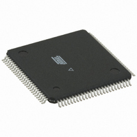
ATMEGA128RZBV-8AU Atmel, ATMEGA128RZBV-8AU Datasheet - Page 297

ATMEGA128RZBV-8AU
Manufacturer Part Number
ATMEGA128RZBV-8AU
Description
MCU ATMEGA1280/AT86RF230 100TQFP
Manufacturer
Atmel
Series
ATMEGAr
Datasheets
1.ATMEGA640V-8CU.pdf
(38 pages)
2.ATMEGA640V-8CU.pdf
(444 pages)
3.AT86RF230-ZU.pdf
(98 pages)
Specifications of ATMEGA128RZBV-8AU
Frequency
2.4GHz
Data Rate - Maximum
2Mbps
Modulation Or Protocol
802.15.4 Zigbee
Applications
General Purpose
Power - Output
3dBm
Sensitivity
-101dBm
Voltage - Supply
1.8 V ~ 3.6 V
Data Interface
PCB, Surface Mount
Memory Size
128kB Flash, 4kB EEPROM, 8kB RAM
Antenna Connector
PCB, Surface Mount
Package / Case
100-TQFP
Wireless Frequency
2.4 GHz
Interface Type
JTAG, SPI
Output Power
3 dBm
For Use With
ATAVRISP2 - PROGRAMMER AVR IN SYSTEMATSTK501 - ADAPTER KIT FOR 64PIN AVR MCUATSTK500 - PROGRAMMER AVR STARTER KIT
Lead Free Status / RoHS Status
Lead free / RoHS Compliant
Operating Temperature
-
Current - Transmitting
-
Current - Receiving
-
Lead Free Status / Rohs Status
Lead free / RoHS Compliant
For Use With/related Products
ATmega128
- Current page: 297 of 444
- Download datasheet (10Mb)
Figure 26-1. Block Diagram
26.3
2549M–AVR–09/10
TDI
TDO
TCK
TMS
TAP - Test Access Port
CONTROLLER
M
U
X
TAP
DEVICE BOUNDARY
INSTRUCTION
BREAKPOINT
SCAN CHAIN
REGISTER
REGISTER
REGISTER
BYPASS
ID
The JTAG interface is accessed through four of the AVR’s pins. In JTAG terminology, these pins
constitute the Test Access Port – TAP. These pins are:
•
•
•
•
The IEEE std. 1149.1 also specifies an optional TAP signal; TRST – Test ReSeT – which is not
provided.
When the JTAGEN Fuse is unprogrammed, these four TAP pins are normal port pins, and the
TAP controller is in reset. When programmed, the input TAP signals are internally pulled high
and the JTAG is enabled for Boundary-scan and programming. The device is shipped with this
fuse programmed.
For the On-chip Debug system, in addition to the JTAG interface pins, the RESET pin is moni-
tored by the debugger to be able to detect external reset sources. The debugger can also pull
the RESET pin low to reset the whole system, assuming only open collectors on the reset line
are used in the application.
DECODER
ADDRESS
TMS: Test mode select. This pin is used for navigating through the TAP-controller state
machine.
TCK: Test Clock. JTAG operation is synchronous to TCK.
TDI: Test Data In. Serial input data to be shifted in to the Instruction Register or Data
Register (Scan Chains).
TDO: Test Data Out. Serial output data from Instruction Register or Data Register.
JTAG PROGRAMMING
MEMORY
FLASH
AND CONTROL
BREAKPOINT
OCD STATUS
INTERFACE
UNIT
Address
Data
I/O PORT 0
I/O PORT n
INTERNAL
FLOW CONTROL
CHAIN
SCAN
ATmega640/1280/1281/2560/2561
UNIT
BOUNDARY SCAN CHAIN
PC
Instruction
JTAG / AVR CORE
COMMUNICATION
PERIPHERAL
INTERFACE
AVR CPU
DIGITAL
UNITS
PERIPHERIAL
ANALOG
UNITS
Control & Clock lines
Analog inputs
297
Related parts for ATMEGA128RZBV-8AU
Image
Part Number
Description
Manufacturer
Datasheet
Request
R

Part Number:
Description:
Manufacturer:
ATMEL Corporation
Datasheet:

Part Number:
Description:
Microcontroller with 128K bytes In-system programmable flash, 8 MHz, power supply =2.7 - 5.5V
Manufacturer:
ATMEL Corporation
Datasheet:

Part Number:
Description:
IC AVR MCU 128K 16MHZ 5V 64TQFP
Manufacturer:
Atmel
Datasheet:

Part Number:
Description:
IC AVR MCU 128K 16MHZ 5V 64-QFN
Manufacturer:
Atmel
Datasheet:

Part Number:
Description:
IC AVR MCU 128K 16MHZ COM 64-QFN
Manufacturer:
Atmel
Datasheet:

Part Number:
Description:
IC AVR MCU 128K 16MHZ 64-TQFP
Manufacturer:
Atmel
Datasheet:

Part Number:
Description:
IC AVR MCU 128K 16MHZ 64-TQFP
Manufacturer:
Atmel
Datasheet:

Part Number:
Description:
IC AVR MCU 128K 16MHZ IND 64-QFN
Manufacturer:
Atmel
Datasheet:

Part Number:
Description:
MCU AVR 128KB FLASH 16MHZ 64TQFP
Manufacturer:
Atmel
Datasheet:

Part Number:
Description:
MCU AVR 128KB FLASH 16MHZ 64QFN
Manufacturer:
Atmel
Datasheet:

Part Number:
Description:
MCU AVR 128KB FLASH 16MHZ 64TQFP
Manufacturer:
Atmel
Datasheet:


