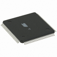
ATMEGA128RZBV-8AU Atmel, ATMEGA128RZBV-8AU Datasheet - Page 21

ATMEGA128RZBV-8AU
Manufacturer Part Number
ATMEGA128RZBV-8AU
Description
MCU ATMEGA1280/AT86RF230 100TQFP
Manufacturer
Atmel
Series
ATMEGAr
Datasheets
1.ATMEGA640V-8CU.pdf
(38 pages)
2.ATMEGA640V-8CU.pdf
(444 pages)
3.AT86RF230-ZU.pdf
(98 pages)
Specifications of ATMEGA128RZBV-8AU
Frequency
2.4GHz
Data Rate - Maximum
2Mbps
Modulation Or Protocol
802.15.4 Zigbee
Applications
General Purpose
Power - Output
3dBm
Sensitivity
-101dBm
Voltage - Supply
1.8 V ~ 3.6 V
Data Interface
PCB, Surface Mount
Memory Size
128kB Flash, 4kB EEPROM, 8kB RAM
Antenna Connector
PCB, Surface Mount
Package / Case
100-TQFP
Wireless Frequency
2.4 GHz
Interface Type
JTAG, SPI
Output Power
3 dBm
For Use With
ATAVRISP2 - PROGRAMMER AVR IN SYSTEMATSTK501 - ADAPTER KIT FOR 64PIN AVR MCUATSTK500 - PROGRAMMER AVR STARTER KIT
Lead Free Status / RoHS Status
Lead free / RoHS Compliant
Operating Temperature
-
Current - Transmitting
-
Current - Receiving
-
Lead Free Status / Rohs Status
Lead free / RoHS Compliant
For Use With/related Products
ATmega128
- Current page: 21 of 444
- Download datasheet (10Mb)
7. AVR Memories
7.1
7.2
2549M–AVR–09/10
In-System Reprogrammable Flash Program Memory
SRAM Data Memory
This section describes the different memories in the ATmega640/1280/1281/2560/2561. The
AVR architecture has two main memory spaces, the Data Memory and the Program Memory
space. In addition, the ATmega640/1280/1281/2560/2561 features an EEPROM Memory for
data storage. All three memory spaces are linear and regular.
The ATmega640/1280/1281/2560/2561 contains 64K/128K/256K bytes On-chip In-System
Reprogrammable Flash memory for program storage, see
are 16 bit or 32 bit wide, the Flash is organized as 32K/64K/128K × 16. For software security,
the Flash Program memory space is divided into two sections, Boot Program section and Appli-
cation Program section.
The Flash memory has an endurance of at least 10,000 write/erase cycles. The
ATmega640/1280/1281/2560/2561 Program Counter (PC) is 15/16/17 bits wide, thus addressing
the 32K/64K/128K program memory locations. The operation of Boot Program section and asso-
ciated Boot Lock bits for software protection are described in detail in
Read-While-Write Self-Programming” on page
tains a detailed description on Flash data serial downloading using the SPI pins or the JTAG
interface.
Constant tables can be allocated within the entire program memory address space (see the LPM
– Load Program Memory instruction description and ELPM - Extended Load Program Memory
instruction description).
Timing diagrams for instruction fetch and execution are presented in
ing” on page
Figure 7-1.
Figure 7-2 on page 23
organized.
The ATmega640/1280/1281/2560/2561 is a complex microcontroller with more peripheral units
than can be supported within the 64 location reserved in the Opcode for the IN and OUT instruc-
tions. For the Extended I/O space from $060 - $1FF in SRAM, only the ST/STS/STD and
LD/LDS/LDD instructions can be used.
The first 4,608/8,704 Data Memory locations address both the Register File, the I/O Memory,
Extended I/O Memory, and the internal data SRAM. The first 32 locations address the Register
file, the next 64 location the standard I/O Memory, then 416 locations of Extended I/O memory
and the next 8,192 locations address the internal data SRAM.
0x7FFF/0xFFFF/0x1FFFF
Address (HEX)
17.
Program Flash Memory Map
shows how the ATmega640/1280/1281/2560/2561 SRAM Memory is
0
ATmega640/1280/1281/2560/2561
Application Flash Section
Boot Flash Section
317.
“Memory Programming” on page 335
Figure
7-1. Since all AVR instructions
“Instruction Execution Tim-
“Boot Loader Support –
con-
21
Related parts for ATMEGA128RZBV-8AU
Image
Part Number
Description
Manufacturer
Datasheet
Request
R

Part Number:
Description:
Manufacturer:
ATMEL Corporation
Datasheet:

Part Number:
Description:
Microcontroller with 128K bytes In-system programmable flash, 8 MHz, power supply =2.7 - 5.5V
Manufacturer:
ATMEL Corporation
Datasheet:

Part Number:
Description:
IC AVR MCU 128K 16MHZ 5V 64TQFP
Manufacturer:
Atmel
Datasheet:

Part Number:
Description:
IC AVR MCU 128K 16MHZ 5V 64-QFN
Manufacturer:
Atmel
Datasheet:

Part Number:
Description:
IC AVR MCU 128K 16MHZ COM 64-QFN
Manufacturer:
Atmel
Datasheet:

Part Number:
Description:
IC AVR MCU 128K 16MHZ 64-TQFP
Manufacturer:
Atmel
Datasheet:

Part Number:
Description:
IC AVR MCU 128K 16MHZ 64-TQFP
Manufacturer:
Atmel
Datasheet:

Part Number:
Description:
IC AVR MCU 128K 16MHZ IND 64-QFN
Manufacturer:
Atmel
Datasheet:

Part Number:
Description:
MCU AVR 128KB FLASH 16MHZ 64TQFP
Manufacturer:
Atmel
Datasheet:

Part Number:
Description:
MCU AVR 128KB FLASH 16MHZ 64QFN
Manufacturer:
Atmel
Datasheet:

Part Number:
Description:
MCU AVR 128KB FLASH 16MHZ 64TQFP
Manufacturer:
Atmel
Datasheet:


