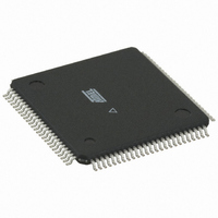
ATMEGA128RZBV-8AU Atmel, ATMEGA128RZBV-8AU Datasheet - Page 277

ATMEGA128RZBV-8AU
Manufacturer Part Number
ATMEGA128RZBV-8AU
Description
MCU ATMEGA1280/AT86RF230 100TQFP
Manufacturer
Atmel
Series
ATMEGAr
Datasheets
1.ATMEGA640V-8CU.pdf
(38 pages)
2.ATMEGA640V-8CU.pdf
(444 pages)
3.AT86RF230-ZU.pdf
(98 pages)
Specifications of ATMEGA128RZBV-8AU
Frequency
2.4GHz
Data Rate - Maximum
2Mbps
Modulation Or Protocol
802.15.4 Zigbee
Applications
General Purpose
Power - Output
3dBm
Sensitivity
-101dBm
Voltage - Supply
1.8 V ~ 3.6 V
Data Interface
PCB, Surface Mount
Memory Size
128kB Flash, 4kB EEPROM, 8kB RAM
Antenna Connector
PCB, Surface Mount
Package / Case
100-TQFP
Wireless Frequency
2.4 GHz
Interface Type
JTAG, SPI
Output Power
3 dBm
For Use With
ATAVRISP2 - PROGRAMMER AVR IN SYSTEMATSTK501 - ADAPTER KIT FOR 64PIN AVR MCUATSTK500 - PROGRAMMER AVR STARTER KIT
Lead Free Status / RoHS Status
Lead free / RoHS Compliant
Operating Temperature
-
Current - Transmitting
-
Current - Receiving
-
Lead Free Status / Rohs Status
Lead free / RoHS Compliant
For Use With/related Products
ATmega128
- Current page: 277 of 444
- Download datasheet (10Mb)
25.3
2549M–AVR–09/10
Starting a Conversion
If differential channels are selected, the voltage difference between the selected input channel
pair then becomes the analog input to the ADC. If single ended channels are used, the amplifier
is bypassed altogether.
The ADC is enabled by setting the ADC Enable bit, ADEN in ADCSRA. Voltage reference and
input channel selections will not go into effect until ADEN is set. The ADC does not consume
power when ADEN is cleared, so it is recommended to switch off the ADC before entering power
saving sleep modes.
The ADC generates a 10-bit result which is presented in the ADC Data Registers, ADCH and
ADCL. By default, the result is presented right adjusted, but can optionally be presented left
adjusted by setting the ADLAR bit in ADMUX.
If the result is left adjusted and no more than 8-bit precision is required, it is sufficient to read
ADCH. Otherwise, ADCL must be read first, then ADCH, to ensure that the content of the Data
Registers belongs to the same conversion. Once ADCL is read, ADC access to Data Registers
is blocked. This means that if ADCL has been read, and a conversion completes before ADCH is
read, neither register is updated and the result from the conversion is lost. When ADCH is read,
ADC access to the ADCH and ADCL Registers is re-enabled.
The ADC has its own interrupt which can be triggered when a conversion completes. When ADC
access to the Data Registers is prohibited between reading of ADCH and ADCL, the interrupt
will trigger even if the result is lost.
A single conversion is started by writing a logical one to the ADC Start Conversion bit, ADSC.
This bit stays high as long as the conversion is in progress and will be cleared by hardware
when the conversion is completed. If a different data channel is selected while a conversion is in
progress, the ADC will finish the current conversion before performing the channel change.
Alternatively, a conversion can be triggered automatically by various sources. Auto Triggering is
enabled by setting the ADC Auto Trigger Enable bit, ADATE in ADCSRA. The trigger source is
selected by setting the ADC Trigger Select bits, ADTS in ADCSRB (See description of the ADTS
bits for a list of the trigger sources). When a positive edge occurs on the selected trigger signal,
the ADC prescaler is reset and a conversion is started. This provides a method of starting con-
versions at fixed intervals. If the trigger signal still is set when the conversion completes, a new
conversion will not be started. If another positive edge occurs on the trigger signal during con-
version, the edge will be ignored. Note that an Interrupt Flag will be set even if the specific
interrupt is disabled or the Global Interrupt Enable bit in SREG is cleared. A conversion can thus
be triggered without causing an interrupt. However, the Interrupt Flag must be cleared in order to
trigger a new conversion at the next interrupt event.
ATmega640/1280/1281/2560/2561
277
Related parts for ATMEGA128RZBV-8AU
Image
Part Number
Description
Manufacturer
Datasheet
Request
R

Part Number:
Description:
Manufacturer:
ATMEL Corporation
Datasheet:

Part Number:
Description:
Microcontroller with 128K bytes In-system programmable flash, 8 MHz, power supply =2.7 - 5.5V
Manufacturer:
ATMEL Corporation
Datasheet:

Part Number:
Description:
IC AVR MCU 128K 16MHZ 5V 64TQFP
Manufacturer:
Atmel
Datasheet:

Part Number:
Description:
IC AVR MCU 128K 16MHZ 5V 64-QFN
Manufacturer:
Atmel
Datasheet:

Part Number:
Description:
IC AVR MCU 128K 16MHZ COM 64-QFN
Manufacturer:
Atmel
Datasheet:

Part Number:
Description:
IC AVR MCU 128K 16MHZ 64-TQFP
Manufacturer:
Atmel
Datasheet:

Part Number:
Description:
IC AVR MCU 128K 16MHZ 64-TQFP
Manufacturer:
Atmel
Datasheet:

Part Number:
Description:
IC AVR MCU 128K 16MHZ IND 64-QFN
Manufacturer:
Atmel
Datasheet:

Part Number:
Description:
MCU AVR 128KB FLASH 16MHZ 64TQFP
Manufacturer:
Atmel
Datasheet:

Part Number:
Description:
MCU AVR 128KB FLASH 16MHZ 64QFN
Manufacturer:
Atmel
Datasheet:

Part Number:
Description:
MCU AVR 128KB FLASH 16MHZ 64TQFP
Manufacturer:
Atmel
Datasheet:


