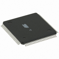
ATMEGA128RZBV-8AU Atmel, ATMEGA128RZBV-8AU Datasheet - Page 148

ATMEGA128RZBV-8AU
Manufacturer Part Number
ATMEGA128RZBV-8AU
Description
MCU ATMEGA1280/AT86RF230 100TQFP
Manufacturer
Atmel
Series
ATMEGAr
Datasheets
1.ATMEGA640V-8CU.pdf
(38 pages)
2.ATMEGA640V-8CU.pdf
(444 pages)
3.AT86RF230-ZU.pdf
(98 pages)
Specifications of ATMEGA128RZBV-8AU
Frequency
2.4GHz
Data Rate - Maximum
2Mbps
Modulation Or Protocol
802.15.4 Zigbee
Applications
General Purpose
Power - Output
3dBm
Sensitivity
-101dBm
Voltage - Supply
1.8 V ~ 3.6 V
Data Interface
PCB, Surface Mount
Memory Size
128kB Flash, 4kB EEPROM, 8kB RAM
Antenna Connector
PCB, Surface Mount
Package / Case
100-TQFP
Wireless Frequency
2.4 GHz
Interface Type
JTAG, SPI
Output Power
3 dBm
For Use With
ATAVRISP2 - PROGRAMMER AVR IN SYSTEMATSTK501 - ADAPTER KIT FOR 64PIN AVR MCUATSTK500 - PROGRAMMER AVR STARTER KIT
Lead Free Status / RoHS Status
Lead free / RoHS Compliant
Operating Temperature
-
Current - Transmitting
-
Current - Receiving
-
Lead Free Status / Rohs Status
Lead free / RoHS Compliant
For Use With/related Products
ATmega128
- Current page: 148 of 444
- Download datasheet (10Mb)
16.9
Table 16-2.
2549M–AVR–09/10
Mode
10
11
12
13
14
15
0
1
2
3
4
5
6
7
8
9
Modes of Operation
WGMn3
0
0
0
0
0
0
0
0
1
1
1
1
1
1
1
1
Waveform Generation Mode Bit Description
WGMn2
(CTCn)
0
0
0
0
1
1
1
1
0
0
0
0
1
1
1
1
non-PWM modes refer to
page
page
A change of the COMnx1:0 bits state will have effect at the first compare match after the bits are
written. For non-PWM modes, the action can be forced to have immediate effect by using the
FOCnx strobe bits.
The mode of operation, that is, the behavior of the Timer/Counter and the Output Compare pins,
is defined by the combination of the Waveform Generation mode (WGMn3:0) and Compare Out-
put mode (COMnx1:0) bits. The Compare Output mode bits do not affect the counting sequence,
while the Waveform Generation mode bits do. The COMnx1:0 bits control whether the PWM out-
put generated should be inverted or not (inverted or non-inverted PWM). For non-PWM modes
the COMnx1:0 bits control whether the output should be set, cleared or toggle at a compare
match.
Note:
For detailed timing information refer to
159, and for phase correct and phase and frequency correct PWM refer to
160.
(PWMn1)
WGMn1
See “Compare Match Output Unit” on page 147.
1. The CTCn and PWMn1:0 bit definition names are obsolete. Use the
0
0
1
1
0
0
1
1
0
0
1
1
0
0
1
1
However, the functionality and location of these bits are compatible with previous versions of
the timer.
(PWMn0)
WGMn0
0
1
0
1
0
1
0
1
0
1
0
1
0
1
0
1
Table 16-3 on page
PWM, Phase and Frequency
PWM, Phase Correct, 10-bit
PWM,Phase and Frequency
PWM, Phase Correct, 8-bit
PWM, Phase Correct, 9-bit
(1)
ATmega640/1280/1281/2560/2561
PWM, Phase Correct
PWM, Phase Correct
Mode of Operation
Fast PWM, 10-bit
Fast PWM, 8-bit
Fast PWM, 9-bit
Timer/Counter
(Reserved)
Fast PWM
Fast PWM
“Timer/Counter Timing Diagrams” on page
Normal
Correct
Correct
CTC
CTC
159. For fast PWM mode refer to
0xFFFF
OCRnA
OCRnA
0x00FF
0x01FF
0x03FF
0x00FF
0x01FF
0x03FF
OCRnA
OCRnA
ICRn
ICRn
ICRn
ICRn
TOP
–
Update of
OCRn
Immediate
Immediate
Immediate
BOTTOM
BOTTOM
BOTTOM
BOTTOM
BOTTOM
BOTTOM
BOTTOM
WGM
TOP
TOP
TOP
TOP
TOP
–
x
at
n2:0 definitions.
Table 16-4 on
Table 16-5 on
156.
TOVn Flag
BOTTOM
BOTTOM
BOTTOM
BOTTOM
BOTTOM
BOTTOM
BOTTOM
Set on
MAX
MAX
MAX
TOP
TOP
TOP
TOP
TOP
–
148
Related parts for ATMEGA128RZBV-8AU
Image
Part Number
Description
Manufacturer
Datasheet
Request
R

Part Number:
Description:
Manufacturer:
ATMEL Corporation
Datasheet:

Part Number:
Description:
Microcontroller with 128K bytes In-system programmable flash, 8 MHz, power supply =2.7 - 5.5V
Manufacturer:
ATMEL Corporation
Datasheet:

Part Number:
Description:
IC AVR MCU 128K 16MHZ 5V 64TQFP
Manufacturer:
Atmel
Datasheet:

Part Number:
Description:
IC AVR MCU 128K 16MHZ 5V 64-QFN
Manufacturer:
Atmel
Datasheet:

Part Number:
Description:
IC AVR MCU 128K 16MHZ COM 64-QFN
Manufacturer:
Atmel
Datasheet:

Part Number:
Description:
IC AVR MCU 128K 16MHZ 64-TQFP
Manufacturer:
Atmel
Datasheet:

Part Number:
Description:
IC AVR MCU 128K 16MHZ 64-TQFP
Manufacturer:
Atmel
Datasheet:

Part Number:
Description:
IC AVR MCU 128K 16MHZ IND 64-QFN
Manufacturer:
Atmel
Datasheet:

Part Number:
Description:
MCU AVR 128KB FLASH 16MHZ 64TQFP
Manufacturer:
Atmel
Datasheet:

Part Number:
Description:
MCU AVR 128KB FLASH 16MHZ 64QFN
Manufacturer:
Atmel
Datasheet:

Part Number:
Description:
MCU AVR 128KB FLASH 16MHZ 64TQFP
Manufacturer:
Atmel
Datasheet:


