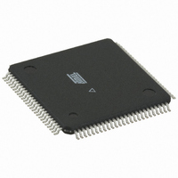
ATMEGA128RZBV-8AU Atmel, ATMEGA128RZBV-8AU Datasheet - Page 172

ATMEGA128RZBV-8AU
Manufacturer Part Number
ATMEGA128RZBV-8AU
Description
MCU ATMEGA1280/AT86RF230 100TQFP
Manufacturer
Atmel
Series
ATMEGAr
Datasheets
1.ATMEGA640V-8CU.pdf
(38 pages)
2.ATMEGA640V-8CU.pdf
(444 pages)
3.AT86RF230-ZU.pdf
(98 pages)
Specifications of ATMEGA128RZBV-8AU
Frequency
2.4GHz
Data Rate - Maximum
2Mbps
Modulation Or Protocol
802.15.4 Zigbee
Applications
General Purpose
Power - Output
3dBm
Sensitivity
-101dBm
Voltage - Supply
1.8 V ~ 3.6 V
Data Interface
PCB, Surface Mount
Memory Size
128kB Flash, 4kB EEPROM, 8kB RAM
Antenna Connector
PCB, Surface Mount
Package / Case
100-TQFP
Wireless Frequency
2.4 GHz
Interface Type
JTAG, SPI
Output Power
3 dBm
For Use With
ATAVRISP2 - PROGRAMMER AVR IN SYSTEMATSTK501 - ADAPTER KIT FOR 64PIN AVR MCUATSTK500 - PROGRAMMER AVR STARTER KIT
Lead Free Status / RoHS Status
Lead free / RoHS Compliant
Operating Temperature
-
Current - Transmitting
-
Current - Receiving
-
Lead Free Status / Rohs Status
Lead free / RoHS Compliant
For Use With/related Products
ATmega128
- Current page: 172 of 444
- Download datasheet (10Mb)
18. Output Compare Modulator (OCM1C0A)
18.1
18.2
2549M–AVR–09/10
Overview
Description
The Output Compare Modulator (OCM) allows generation of waveforms modulated with a carrier
frequency. The modulator uses the outputs from the Output Compare Unit C of the 16-bit
Timer/Counter1 and the Output Compare Unit of the 8-bit Timer/Counter0. For more details
about these Timer/Counters see
bit Timer/Counter2 with PWM and Asynchronous Operation” on page
Figure 18-1. Output Compare Modulator, Block Diagram
When the modulator is enabled, the two output compare channels are modulated together as
shown in the block diagram (see
The Output Compare unit 1C and Output Compare unit 2 shares the PB7 port pin for output. The
outputs of the Output Compare units (OC1C and OC0A) overrides the normal PORTB7 Register
when one of them is enabled (that is, when COMnx1:0 is not equal to zero). When both OC1C
and OC0A are enabled at the same time, the modulator is automatically enabled.
The functional equivalent schematic of the modulator is shown on
includes part of the Timer/Counter units and the port B pin 7 output driver circuit.
Figure 18-2. Output Compare Modulator, Schematic
( From Waveform Generator )
( From Waveform Generator )
COMA01
COMA00
COM1C1
COM1C0
Timer/Counter 1
Timer/Counter 0
PORTB7
D
OC1C
D
OC0A
D
Q
Q
Q
ATmega640/1280/1281/2560/2561
“Timer/Counter 0, 1, 3, 4, and 5 Prescaler” on page 169
Figure
DATABUS
18-1).
OC1C
OC0A
Modulator
0
1
DDRB7
D
Figure
Q
1
0
174.
OC0A / PB7
OC1C /
18-2. The schematic
Pin
Vcc
OC0A/ PB7
and
OC1C /
Pin
172
“8-
Related parts for ATMEGA128RZBV-8AU
Image
Part Number
Description
Manufacturer
Datasheet
Request
R

Part Number:
Description:
Manufacturer:
ATMEL Corporation
Datasheet:

Part Number:
Description:
Microcontroller with 128K bytes In-system programmable flash, 8 MHz, power supply =2.7 - 5.5V
Manufacturer:
ATMEL Corporation
Datasheet:

Part Number:
Description:
IC AVR MCU 128K 16MHZ 5V 64TQFP
Manufacturer:
Atmel
Datasheet:

Part Number:
Description:
IC AVR MCU 128K 16MHZ 5V 64-QFN
Manufacturer:
Atmel
Datasheet:

Part Number:
Description:
IC AVR MCU 128K 16MHZ COM 64-QFN
Manufacturer:
Atmel
Datasheet:

Part Number:
Description:
IC AVR MCU 128K 16MHZ 64-TQFP
Manufacturer:
Atmel
Datasheet:

Part Number:
Description:
IC AVR MCU 128K 16MHZ 64-TQFP
Manufacturer:
Atmel
Datasheet:

Part Number:
Description:
IC AVR MCU 128K 16MHZ IND 64-QFN
Manufacturer:
Atmel
Datasheet:

Part Number:
Description:
MCU AVR 128KB FLASH 16MHZ 64TQFP
Manufacturer:
Atmel
Datasheet:

Part Number:
Description:
MCU AVR 128KB FLASH 16MHZ 64QFN
Manufacturer:
Atmel
Datasheet:

Part Number:
Description:
MCU AVR 128KB FLASH 16MHZ 64TQFP
Manufacturer:
Atmel
Datasheet:


