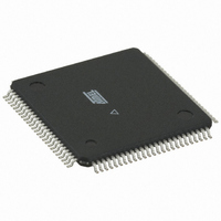
ATMEGA128RZBV-8AU Atmel, ATMEGA128RZBV-8AU Datasheet - Page 22

ATMEGA128RZBV-8AU
Manufacturer Part Number
ATMEGA128RZBV-8AU
Description
MCU ATMEGA1280/AT86RF230 100TQFP
Manufacturer
Atmel
Series
ATMEGAr
Datasheets
1.ATMEGA640V-8CU.pdf
(38 pages)
2.ATMEGA640V-8CU.pdf
(444 pages)
3.AT86RF230-ZU.pdf
(98 pages)
Specifications of ATMEGA128RZBV-8AU
Frequency
2.4GHz
Data Rate - Maximum
2Mbps
Modulation Or Protocol
802.15.4 Zigbee
Applications
General Purpose
Power - Output
3dBm
Sensitivity
-101dBm
Voltage - Supply
1.8 V ~ 3.6 V
Data Interface
PCB, Surface Mount
Memory Size
128kB Flash, 4kB EEPROM, 8kB RAM
Antenna Connector
PCB, Surface Mount
Package / Case
100-TQFP
Wireless Frequency
2.4 GHz
Interface Type
JTAG, SPI
Output Power
3 dBm
For Use With
ATAVRISP2 - PROGRAMMER AVR IN SYSTEMATSTK501 - ADAPTER KIT FOR 64PIN AVR MCUATSTK500 - PROGRAMMER AVR STARTER KIT
Lead Free Status / RoHS Status
Lead free / RoHS Compliant
Operating Temperature
-
Current - Transmitting
-
Current - Receiving
-
Lead Free Status / Rohs Status
Lead free / RoHS Compliant
For Use With/related Products
ATmega128
- Current page: 22 of 444
- Download datasheet (10Mb)
ATmega640/1280/1281/2560/2561
An optional external data SRAM can be used with the ATmega640/1280/1281/2560/2561. This
SRAM will occupy an area in the remaining address locations in the 64K address space. This
area starts at the address following the internal SRAM. The Register file, I/O, Extended I/O and
Internal SRAM occupies the lowest 4,608/8,704 bytes, so when using 64 Kbytes (65,536 bytes)
of External Memory, 60,478/56,832 Bytes of External Memory are available. See
“External
Memory Interface” on page 28
for details on how to take advantage of the external memory map.
When the addresses accessing the SRAM memory space exceeds the internal data memory
locations, the external data SRAM is accessed using the same instructions as for the internal
data memory access. When the internal data memories are accessed, the read and write strobe
pins (PG0 and PG1) are inactive during the whole access cycle. External SRAM operation is
enabled by setting the SRE bit in the XMCRA Register.
Accessing external SRAM takes one additional clock cycle per byte compared to access of the
internal SRAM. This means that the commands LD, ST, LDS, STS, LDD, STD, PUSH, and POP
take one additional clock cycle. If the Stack is placed in external SRAM, interrupts, subroutine
calls and returns take three clock cycles extra because the three-byte program counter is
pushed and popped, and external memory access does not take advantage of the internal pipe-
line memory access. When external SRAM interface is used with wait-state, one-byte external
access takes two, three, or four additional clock cycles for one, two, and three wait-states
respectively. Interrupts, subroutine calls and returns will need five, seven, or nine clock cycles
more than specified in the instruction set manual for one, two, and three wait-states.
The five different addressing modes for the data memory cover: Direct, Indirect with Displace-
ment, Indirect, Indirect with Pre-decrement, and Indirect with Post-increment. In the Register file,
registers R26 to R31 feature the indirect addressing pointer registers.
The direct addressing reaches the entire data space.
The Indirect with Displacement mode reaches 63 address locations from the base address given
by the Y- or Z-register.
When using register indirect addressing modes with automatic pre-decrement and post-incre-
ment, the address registers X, Y, and Z are decremented or incremented.
The 32 general purpose working registers, 64 I/O registers, and the 4,196/8,192 bytes of internal
data SRAM in the ATmega640/1280/1281/2560/2561 are all accessible through all these
addressing modes. The Register File is described in
“General Purpose Register File” on page
15.
22
2549M–AVR–09/10
Related parts for ATMEGA128RZBV-8AU
Image
Part Number
Description
Manufacturer
Datasheet
Request
R

Part Number:
Description:
Manufacturer:
ATMEL Corporation
Datasheet:

Part Number:
Description:
Microcontroller with 128K bytes In-system programmable flash, 8 MHz, power supply =2.7 - 5.5V
Manufacturer:
ATMEL Corporation
Datasheet:

Part Number:
Description:
IC AVR MCU 128K 16MHZ 5V 64TQFP
Manufacturer:
Atmel
Datasheet:

Part Number:
Description:
IC AVR MCU 128K 16MHZ 5V 64-QFN
Manufacturer:
Atmel
Datasheet:

Part Number:
Description:
IC AVR MCU 128K 16MHZ COM 64-QFN
Manufacturer:
Atmel
Datasheet:

Part Number:
Description:
IC AVR MCU 128K 16MHZ 64-TQFP
Manufacturer:
Atmel
Datasheet:

Part Number:
Description:
IC AVR MCU 128K 16MHZ 64-TQFP
Manufacturer:
Atmel
Datasheet:

Part Number:
Description:
IC AVR MCU 128K 16MHZ IND 64-QFN
Manufacturer:
Atmel
Datasheet:

Part Number:
Description:
MCU AVR 128KB FLASH 16MHZ 64TQFP
Manufacturer:
Atmel
Datasheet:

Part Number:
Description:
MCU AVR 128KB FLASH 16MHZ 64QFN
Manufacturer:
Atmel
Datasheet:

Part Number:
Description:
MCU AVR 128KB FLASH 16MHZ 64TQFP
Manufacturer:
Atmel
Datasheet:


