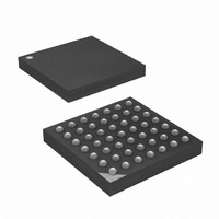
ATXMEGA32A4-CUR Atmel, ATXMEGA32A4-CUR Datasheet - Page 381

ATXMEGA32A4-CUR
Manufacturer Part Number
ATXMEGA32A4-CUR
Description
MCU AVR 32+4 FLASH 49VFBGA
Manufacturer
Atmel
Series
AVR® XMEGAr
Specifications of ATXMEGA32A4-CUR
Core Processor
AVR
Core Size
8/16-Bit
Speed
32MHz
Connectivity
I²C, IrDA, SPI, UART/USART
Peripherals
Brown-out Detect/Reset, DMA, POR, PWM, WDT
Number Of I /o
34
Program Memory Size
32KB (16K x 16)
Program Memory Type
FLASH
Eeprom Size
2K x 8
Ram Size
4K x 8
Voltage - Supply (vcc/vdd)
1.6 V ~ 3.6 V
Data Converters
A/D 12x12b, D/A 2x12b
Oscillator Type
Internal
Operating Temperature
-40°C ~ 85°C
Package / Case
49-VFBGA
For Use With
ATAVRONEKIT - KIT AVR/AVR32 DEBUGGER/PROGRMMRATSTK600 - DEV KIT FOR AVR/AVR32770-1007 - ISP 4PORT ATMEL AVR MCU SPI/JTAG770-1004 - ISP 4PORT FOR ATMEL AVR MCU SPI
Lead Free Status / RoHS Status
Lead free / RoHS Compliant
Available stocks
Company
Part Number
Manufacturer
Quantity
Price
- Current page: 381 of 445
- Download datasheet (6Mb)
30.12.1
30.12.2
30.12.2.1
30.12.2.2
30.12.3
8077H–AVR–12/09
CMD[6:0]
Flash Page Buffer
0x00
0x40
0x43
Enabling External Programming Interface
NVM Programming
NVM Commands
Addressing the NVM
NVM Busy
Commands / Operation
No Operation
Chip Erase
Read NVM
(1)
NVM programming from the PDI requires enabling, and this is one the following fashion.
When the NVMEN bit in the PDI STATUS register is set the NVM interface is active from the
PDI.
When the PDI NVM interface is enabled, all the memories in the device is memory-mapped in
the PDI address space. The PDI controller does not need to access the NVM controller's
address or data registers, but that the NVM controller must be loaded with the correct command
(i.e. to read from any NVM, the controller must be loaded with the NVM Read command before
trying to load data from the PDIBUS address space). For the reminder of this section all refer-
ences to reading and writing data or program memory addresses from PDI, refer to the memory
map as shown in
The PDI is always using byte addressing, hence all memory addresses must be byte addresses.
When filling the Flash or EEPROM page buffers, only the least significant bits of the address are
used to determine locations within the page buffer. Still, the complete memory mapped address
for the Flash or EEPROM page is required to ensure correct address mapping. The user must
pay attention to page boundaries for both page buffer loads and page buffer writes.
During programming (page erase and page write) when the NVM is busy, the complete NVM is
blocked for reading.
The NVM commands that can be used for accessing the NVM memories from external program-
ming are listed in
programming.
For external programming, the Trigger for Action Triggered Commands is to set the CMDEX bit
in the NVM CTRLA register (CMDEX). The Read Triggered Commands are triggered by a direct
or indirect Load instruction (LDS or LD) from the PDI (PDI Read). The Write Triggered Com-
mands is triggered by a direct or indirect Store instruction (STS or ST) from the PDI (PDI Write).
Section 30.12.3.1 on page 383
algorithm for each NVM operation. The commands are protected by the Lock Bits, and if Read
and Write Lock is set, only the Chip Erase and Flash CRC commands are available.
Table 30-5.
1. Load the RESET register in the PDI with 0x59 - the Reset Signature.
2. Load the correct NVM key in the PDI.
3. Poll NVMEN in the PDI Status Register (PDI STATUS) until NVMEN is set.
NVM commands available for external programming
Figure 30-4 on page
Table
30-5. This is a super-set of the commands available for self-
through
380.
Section 30.12.3.11 on page 385
Trigger
-
CMDEX
PDI Read
Change
Protected
explains in detail the
Y
N
-
XMEGA A
NVM Busy
Y
N
-
381
Related parts for ATXMEGA32A4-CUR
Image
Part Number
Description
Manufacturer
Datasheet
Request
R

Part Number:
Description:
DEV KIT FOR AVR/AVR32
Manufacturer:
Atmel
Datasheet:

Part Number:
Description:
INTERVAL AND WIPE/WASH WIPER CONTROL IC WITH DELAY
Manufacturer:
ATMEL Corporation
Datasheet:

Part Number:
Description:
Low-Voltage Voice-Switched IC for Hands-Free Operation
Manufacturer:
ATMEL Corporation
Datasheet:

Part Number:
Description:
MONOLITHIC INTEGRATED FEATUREPHONE CIRCUIT
Manufacturer:
ATMEL Corporation
Datasheet:

Part Number:
Description:
AM-FM Receiver IC U4255BM-M
Manufacturer:
ATMEL Corporation
Datasheet:

Part Number:
Description:
Monolithic Integrated Feature Phone Circuit
Manufacturer:
ATMEL Corporation
Datasheet:

Part Number:
Description:
Multistandard Video-IF and Quasi Parallel Sound Processing
Manufacturer:
ATMEL Corporation
Datasheet:

Part Number:
Description:
High-performance EE PLD
Manufacturer:
ATMEL Corporation
Datasheet:

Part Number:
Description:
8-bit Flash Microcontroller
Manufacturer:
ATMEL Corporation
Datasheet:

Part Number:
Description:
2-Wire Serial EEPROM
Manufacturer:
ATMEL Corporation
Datasheet:


