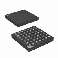
ATXMEGA32A4-CUR Atmel, ATXMEGA32A4-CUR Datasheet - Page 24

ATXMEGA32A4-CUR
Manufacturer Part Number
ATXMEGA32A4-CUR
Description
MCU AVR 32+4 FLASH 49VFBGA
Manufacturer
Atmel
Series
AVR® XMEGAr
Specifications of ATXMEGA32A4-CUR
Core Processor
AVR
Core Size
8/16-Bit
Speed
32MHz
Connectivity
I²C, IrDA, SPI, UART/USART
Peripherals
Brown-out Detect/Reset, DMA, POR, PWM, WDT
Number Of I /o
34
Program Memory Size
32KB (16K x 16)
Program Memory Type
FLASH
Eeprom Size
2K x 8
Ram Size
4K x 8
Voltage - Supply (vcc/vdd)
1.6 V ~ 3.6 V
Data Converters
A/D 12x12b, D/A 2x12b
Oscillator Type
Internal
Operating Temperature
-40°C ~ 85°C
Package / Case
49-VFBGA
For Use With
ATAVRONEKIT - KIT AVR/AVR32 DEBUGGER/PROGRMMRATSTK600 - DEV KIT FOR AVR/AVR32770-1007 - ISP 4PORT ATMEL AVR MCU SPI/JTAG770-1004 - ISP 4PORT FOR ATMEL AVR MCU SPI
Lead Free Status / RoHS Status
Lead free / RoHS Compliant
Available stocks
Company
Part Number
Manufacturer
Quantity
Price
- Current page: 24 of 445
- Download datasheet (6Mb)
4.10.1
4.11
4.12
4.13
8077H–AVR–12/09
Memory Timing
Device ID
JTAG Disable
Bus Priority
Figure 4-3.
When several masters request access to the same bus, the bus priority is in the following order
(from higher to lower priority)
Read and write access to the I/O Memory takes one CPU clock cycle. Write to SRAM takes one
cycle and read from SRAM takes two cycles. For burst read (DMA), new data is available every
cycle. EEPROM page load (write) takes one cycle and three cycles are required for read. For
burst read, new data is available every second cycle. External memory has multi-cycle read and
write. The number of cycles depends on type of memory and configuration of the External Bus
Interface. Refer to the instruction summary for more details on instructions and instruction
timing.
Each device has a three-byte device ID which identifies the device. These registers identify
Atmel as the manufacturer of the device and the device type. A separate register contains the
revision number of the device.
It is possible to disable the JTAG interface from the application software. This will prevent all
external JTAG access to the memory, until the next device reset or if JTAG is enabled again
1. Bus Master with ongoing access
2. Bus Master with ongoing burst
3. Bus Master requesting burst access
4. Bus Master requesting bus access
a. Alternating DMA Controller Read and DMA Controller Write when the they access
a. CPU has priority
a. CPU has priority
the same Data Memory section.
DMA Controller
DMA Controller
Bus Access
Read
Write
CPU
Data Memory Bus
I/O Memory
EEPROM
External
Memory
SRAM
XMEGA A
24
Related parts for ATXMEGA32A4-CUR
Image
Part Number
Description
Manufacturer
Datasheet
Request
R

Part Number:
Description:
DEV KIT FOR AVR/AVR32
Manufacturer:
Atmel
Datasheet:

Part Number:
Description:
INTERVAL AND WIPE/WASH WIPER CONTROL IC WITH DELAY
Manufacturer:
ATMEL Corporation
Datasheet:

Part Number:
Description:
Low-Voltage Voice-Switched IC for Hands-Free Operation
Manufacturer:
ATMEL Corporation
Datasheet:

Part Number:
Description:
MONOLITHIC INTEGRATED FEATUREPHONE CIRCUIT
Manufacturer:
ATMEL Corporation
Datasheet:

Part Number:
Description:
AM-FM Receiver IC U4255BM-M
Manufacturer:
ATMEL Corporation
Datasheet:

Part Number:
Description:
Monolithic Integrated Feature Phone Circuit
Manufacturer:
ATMEL Corporation
Datasheet:

Part Number:
Description:
Multistandard Video-IF and Quasi Parallel Sound Processing
Manufacturer:
ATMEL Corporation
Datasheet:

Part Number:
Description:
High-performance EE PLD
Manufacturer:
ATMEL Corporation
Datasheet:

Part Number:
Description:
8-bit Flash Microcontroller
Manufacturer:
ATMEL Corporation
Datasheet:

Part Number:
Description:
2-Wire Serial EEPROM
Manufacturer:
ATMEL Corporation
Datasheet:


