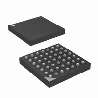
ATXMEGA32A4-CUR Atmel, ATXMEGA32A4-CUR Datasheet - Page 297

ATXMEGA32A4-CUR
Manufacturer Part Number
ATXMEGA32A4-CUR
Description
MCU AVR 32+4 FLASH 49VFBGA
Manufacturer
Atmel
Series
AVR® XMEGAr
Specifications of ATXMEGA32A4-CUR
Core Processor
AVR
Core Size
8/16-Bit
Speed
32MHz
Connectivity
I²C, IrDA, SPI, UART/USART
Peripherals
Brown-out Detect/Reset, DMA, POR, PWM, WDT
Number Of I /o
34
Program Memory Size
32KB (16K x 16)
Program Memory Type
FLASH
Eeprom Size
2K x 8
Ram Size
4K x 8
Voltage - Supply (vcc/vdd)
1.6 V ~ 3.6 V
Data Converters
A/D 12x12b, D/A 2x12b
Oscillator Type
Internal
Operating Temperature
-40°C ~ 85°C
Package / Case
49-VFBGA
For Use With
ATAVRONEKIT - KIT AVR/AVR32 DEBUGGER/PROGRMMRATSTK600 - DEV KIT FOR AVR/AVR32770-1007 - ISP 4PORT ATMEL AVR MCU SPI/JTAG770-1004 - ISP 4PORT FOR ATMEL AVR MCU SPI
Lead Free Status / RoHS Status
Lead free / RoHS Compliant
Available stocks
Company
Part Number
Manufacturer
Quantity
Price
- Current page: 297 of 445
- Download datasheet (6Mb)
25.9.1
25.9.2
8077H–AVR–12/09
Single conversion without gain
Single conversion with gain
RES is the resolution, 8- or 12-bit. The propagation delay will increase by one extra ADC clock
cycle if the Gain Stage (GAIN) is used.
Even though the propagation delay is longer than one ADC clock cycle, the pipelined design
removes any limitations on sample speed versus propagation delay.
Figure 25-13 on page 297
ing of the start conversion bit, or the event triggering the conversion (START), must occur
minimum one peripheral clock cycles before the ADC clock cycle where the conversion actually
start (indicated with the grey slope of the START trigger).
The analog input source is sampled in the first half of the first cycle, and the sample time is
always a half ADC clock period. Using a faster or slower ADC clock and sample rate will affect
the sample time.
The Most Significant Bit (MSB) of the result is converted first, and the rest of the bits are con-
verted during the next 3 (for 8-bit results) or 5 (for 12-bit results) ADC clock cycles. Converting
one bit takes a half ADC clock period. During the last cycle the result is prepared before the
Interrupt Flag is set. The result is available in the Result Register for readout.
Figure 25-13. ADC timing for one single conversion without gain
Figure 25-14 on page 298
the
the gainstage will sample and amplify the analog input source before the ADC samples an con-
verts the amplified analog value. Compared to a single conversion without gain this adds one
ADC clock cycle (between START and ADC Sample) for the gain stage sample and amplify. The
sample time for the gain stage is a half ADC clock cycle.
Propagation Delay =
CONVERTING BIT
”Overview” on page 289
ADC SAMPLE
CLK
START
ADC
IF
1
----------------------------------------- -
1
+
MSB
RES
---------- -
2
f
ADC
shows the ADC timing for one single conversion with gain. As seen in
shows the ADC timing for a single conversion without gain. The writ-
+
10
the gain stage is placed prior to the actual ADC. This means that
GAIN
2
9
8
3
7
6
4
5
4
5
3
2
6
1
LSB
XMEGA A
7
8
297
Related parts for ATXMEGA32A4-CUR
Image
Part Number
Description
Manufacturer
Datasheet
Request
R

Part Number:
Description:
DEV KIT FOR AVR/AVR32
Manufacturer:
Atmel
Datasheet:

Part Number:
Description:
INTERVAL AND WIPE/WASH WIPER CONTROL IC WITH DELAY
Manufacturer:
ATMEL Corporation
Datasheet:

Part Number:
Description:
Low-Voltage Voice-Switched IC for Hands-Free Operation
Manufacturer:
ATMEL Corporation
Datasheet:

Part Number:
Description:
MONOLITHIC INTEGRATED FEATUREPHONE CIRCUIT
Manufacturer:
ATMEL Corporation
Datasheet:

Part Number:
Description:
AM-FM Receiver IC U4255BM-M
Manufacturer:
ATMEL Corporation
Datasheet:

Part Number:
Description:
Monolithic Integrated Feature Phone Circuit
Manufacturer:
ATMEL Corporation
Datasheet:

Part Number:
Description:
Multistandard Video-IF and Quasi Parallel Sound Processing
Manufacturer:
ATMEL Corporation
Datasheet:

Part Number:
Description:
High-performance EE PLD
Manufacturer:
ATMEL Corporation
Datasheet:

Part Number:
Description:
8-bit Flash Microcontroller
Manufacturer:
ATMEL Corporation
Datasheet:

Part Number:
Description:
2-Wire Serial EEPROM
Manufacturer:
ATMEL Corporation
Datasheet:


