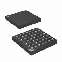
ATXMEGA32A4-CUR Atmel, ATXMEGA32A4-CUR Datasheet - Page 352

ATXMEGA32A4-CUR
Manufacturer Part Number
ATXMEGA32A4-CUR
Description
MCU AVR 32+4 FLASH 49VFBGA
Manufacturer
Atmel
Series
AVR® XMEGAr
Specifications of ATXMEGA32A4-CUR
Core Processor
AVR
Core Size
8/16-Bit
Speed
32MHz
Connectivity
I²C, IrDA, SPI, UART/USART
Peripherals
Brown-out Detect/Reset, DMA, POR, PWM, WDT
Number Of I /o
34
Program Memory Size
32KB (16K x 16)
Program Memory Type
FLASH
Eeprom Size
2K x 8
Ram Size
4K x 8
Voltage - Supply (vcc/vdd)
1.6 V ~ 3.6 V
Data Converters
A/D 12x12b, D/A 2x12b
Oscillator Type
Internal
Operating Temperature
-40°C ~ 85°C
Package / Case
49-VFBGA
For Use With
ATAVRONEKIT - KIT AVR/AVR32 DEBUGGER/PROGRMMRATSTK600 - DEV KIT FOR AVR/AVR32770-1007 - ISP 4PORT ATMEL AVR MCU SPI/JTAG770-1004 - ISP 4PORT FOR ATMEL AVR MCU SPI
Lead Free Status / RoHS Status
Lead free / RoHS Compliant
Available stocks
Company
Part Number
Manufacturer
Quantity
Price
- Current page: 352 of 445
- Download datasheet (6Mb)
29.4.6
29.4.6.1
8077H–AVR–12/09
Serial transmission
Status signalling
Figure 29-12. Changing and sampling data
When data transmission is initiated, a data byte is loaded in parallel into the shift register, and
then serialized by shifting the byte out on TDO. The Parity bit is generated and stitched to the
data byte during transmission. The transmission speed is dictated by the TCK signal.
If the PDI is in TX-mode (as a response to an LD-instruction), and a transmission request from
the PDI Controller is pending when the TAP-controller enters the Capture-DR state, valid data
will be parallel-loaded into the shift-register and a correct Parity bit will be generated and trans-
mitted along with the data byte in the Shift-DR state.
If the PDI is in RX-mode when the TAP-controller enters the Capture-DR state, an EMPTY byte
(0xEB) will be parallel-loaded into the shift-register, and the Parity bit will be set (forcing a parity
error) when data is shifted out in the Shift-DR state. This situation occurs during normal PDI
command - and operand reception.
If the PDI is in TX-mode (as a response to an LD-instruction), but no transmission request from
the PDI Controller is yet pending when the TAP-controller enters the Capture-DR state, a
DELAY byte (0xDB) will be parallel-loaded into the shift-register, and the Parity bit will be set
(forcing a parity error) when data is shifted out in the Shift-DR state. This situation occurs during
data transmission if the data to be transmitted is not yet available.
Figure 29-13 on page 352
a response to the repeated indirect LD instruction. However, in this example the device is not
able to return data bytes faster than one valid byte per two transmitted frames, intermediate
DELAY characters are inserted.
Figure 29-13. Date not ready marking
If a DELAY data frame is transmitted as a response to an LD instruction, the programmer should
interpret this as if the JTAG-interface had no data yet ready for transmission in the previous DR-
Capture state. The proper reaction from the programmer is to initiate repeated transfers until a
valid data byte is received. The LD-instruction is defined to return a specified number of valid
frames, not just a number of frames. Hence if the programmer detects a DELAY Character after
transmitting an LD-instruction, the LD-instruction should not be retransmitted, because the first
LD response would still be pending.
Programmer
External
Commands/data
TD I/TDO
TC K
Device
FRAME 0
shows an uninterrupted flow of data frames from the PDI (Device) as
REP
FRAME 1
CNT
S am ple
LD *(ptr)
FRAME 2
0xDB 1
S am ple
FRAME 0
FRAME 1
D0
P 0xDB 1
S am ple
FRAME 2
XMEGA A
FRAME 3
D1
P
352
Related parts for ATXMEGA32A4-CUR
Image
Part Number
Description
Manufacturer
Datasheet
Request
R

Part Number:
Description:
DEV KIT FOR AVR/AVR32
Manufacturer:
Atmel
Datasheet:

Part Number:
Description:
INTERVAL AND WIPE/WASH WIPER CONTROL IC WITH DELAY
Manufacturer:
ATMEL Corporation
Datasheet:

Part Number:
Description:
Low-Voltage Voice-Switched IC for Hands-Free Operation
Manufacturer:
ATMEL Corporation
Datasheet:

Part Number:
Description:
MONOLITHIC INTEGRATED FEATUREPHONE CIRCUIT
Manufacturer:
ATMEL Corporation
Datasheet:

Part Number:
Description:
AM-FM Receiver IC U4255BM-M
Manufacturer:
ATMEL Corporation
Datasheet:

Part Number:
Description:
Monolithic Integrated Feature Phone Circuit
Manufacturer:
ATMEL Corporation
Datasheet:

Part Number:
Description:
Multistandard Video-IF and Quasi Parallel Sound Processing
Manufacturer:
ATMEL Corporation
Datasheet:

Part Number:
Description:
High-performance EE PLD
Manufacturer:
ATMEL Corporation
Datasheet:

Part Number:
Description:
8-bit Flash Microcontroller
Manufacturer:
ATMEL Corporation
Datasheet:

Part Number:
Description:
2-Wire Serial EEPROM
Manufacturer:
ATMEL Corporation
Datasheet:


