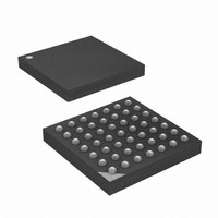
ATXMEGA32A4-CUR Atmel, ATXMEGA32A4-CUR Datasheet - Page 208

ATXMEGA32A4-CUR
Manufacturer Part Number
ATXMEGA32A4-CUR
Description
MCU AVR 32+4 FLASH 49VFBGA
Manufacturer
Atmel
Series
AVR® XMEGAr
Specifications of ATXMEGA32A4-CUR
Core Processor
AVR
Core Size
8/16-Bit
Speed
32MHz
Connectivity
I²C, IrDA, SPI, UART/USART
Peripherals
Brown-out Detect/Reset, DMA, POR, PWM, WDT
Number Of I /o
34
Program Memory Size
32KB (16K x 16)
Program Memory Type
FLASH
Eeprom Size
2K x 8
Ram Size
4K x 8
Voltage - Supply (vcc/vdd)
1.6 V ~ 3.6 V
Data Converters
A/D 12x12b, D/A 2x12b
Oscillator Type
Internal
Operating Temperature
-40°C ~ 85°C
Package / Case
49-VFBGA
For Use With
ATAVRONEKIT - KIT AVR/AVR32 DEBUGGER/PROGRMMRATSTK600 - DEV KIT FOR AVR/AVR32770-1007 - ISP 4PORT ATMEL AVR MCU SPI/JTAG770-1004 - ISP 4PORT FOR ATMEL AVR MCU SPI
Lead Free Status / RoHS Status
Lead free / RoHS Compliant
Available stocks
Company
Part Number
Manufacturer
Quantity
Price
- Current page: 208 of 445
- Download datasheet (6Mb)
19.3.3
19.3.4
19.3.5
19.3.6
8077H–AVR–12/09
Bit Transfer
Address Packet
Data Packet
Transaction
As illustrated by
period of the SCL line. Consequently the SDA value can only be changed during the low period
of the clock. This is ensured in hardware by the TWI module.
Figure 19-4. Data Validity
Combining bit transfers results in the formation of address and data packets. These packets
consist of 8 data bits (one byte) with the most significant bit transferred first, plus a single bit not-
acknowledge (NACK) or acknowledge (ACK) response. The addressed device signals ACK by
pulling the SCL line low, and NACK by leaving the line SCL high during the ninth clock cycle.
After the START condition, a 7-bit address followed by a read/write (R/W) bit is sent. This is
always transmitted by the Master. A slave recognizing its address will ACK the address by pull-
ing the data line low the next SCL cycle, while all other slaves should keep the TWI lines
released, and wait for the next START and address. The 7-bit address, the R/W bit and the
acknowledge bit combined is the address packet. Only one address packet for each START
condition is given, also when 10-bit addressing is used.
The R/W specifies the direction of the transaction. If the R/W bit is low, it indicates a Master
Write transaction, and the master will transmit its data after the slave has acknowledged its
address. Opposite, for a Master Read operation the slave will start to transmit data after
acknowledging its address.
Data packets succeed an address packet or another data packet. All data packets are nine bits
long, consisting of one data byte and an acknowledge bit. The direction bit in the previous
address packet determines the direction in which the data is transferred.
A transaction is the complete transfer from a START to a STOP condition, including any
Repeated START conditions in between. The TWI standard defines three fundamental transac-
tion modes: Master Write, Master Read, and combined transaction.
Figure 19-5
ing a START condition (S) followed by an address packet with direction bit set to zero
(ADDRESS+W).
SDA
SCL
illustrates the Master Write transaction. The master initiates the transaction by issu-
Figure 19-4
a bit transferred on the SDA line must be stable for the entire high
DATA
Valid
Change
Allowed
XMEGA A
208
Related parts for ATXMEGA32A4-CUR
Image
Part Number
Description
Manufacturer
Datasheet
Request
R

Part Number:
Description:
DEV KIT FOR AVR/AVR32
Manufacturer:
Atmel
Datasheet:

Part Number:
Description:
INTERVAL AND WIPE/WASH WIPER CONTROL IC WITH DELAY
Manufacturer:
ATMEL Corporation
Datasheet:

Part Number:
Description:
Low-Voltage Voice-Switched IC for Hands-Free Operation
Manufacturer:
ATMEL Corporation
Datasheet:

Part Number:
Description:
MONOLITHIC INTEGRATED FEATUREPHONE CIRCUIT
Manufacturer:
ATMEL Corporation
Datasheet:

Part Number:
Description:
AM-FM Receiver IC U4255BM-M
Manufacturer:
ATMEL Corporation
Datasheet:

Part Number:
Description:
Monolithic Integrated Feature Phone Circuit
Manufacturer:
ATMEL Corporation
Datasheet:

Part Number:
Description:
Multistandard Video-IF and Quasi Parallel Sound Processing
Manufacturer:
ATMEL Corporation
Datasheet:

Part Number:
Description:
High-performance EE PLD
Manufacturer:
ATMEL Corporation
Datasheet:

Part Number:
Description:
8-bit Flash Microcontroller
Manufacturer:
ATMEL Corporation
Datasheet:

Part Number:
Description:
2-Wire Serial EEPROM
Manufacturer:
ATMEL Corporation
Datasheet:


