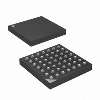
ATXMEGA32A4-CUR Atmel, ATXMEGA32A4-CUR Datasheet - Page 340

ATXMEGA32A4-CUR
Manufacturer Part Number
ATXMEGA32A4-CUR
Description
MCU AVR 32+4 FLASH 49VFBGA
Manufacturer
Atmel
Series
AVR® XMEGAr
Specifications of ATXMEGA32A4-CUR
Core Processor
AVR
Core Size
8/16-Bit
Speed
32MHz
Connectivity
I²C, IrDA, SPI, UART/USART
Peripherals
Brown-out Detect/Reset, DMA, POR, PWM, WDT
Number Of I /o
34
Program Memory Size
32KB (16K x 16)
Program Memory Type
FLASH
Eeprom Size
2K x 8
Ram Size
4K x 8
Voltage - Supply (vcc/vdd)
1.6 V ~ 3.6 V
Data Converters
A/D 12x12b, D/A 2x12b
Oscillator Type
Internal
Operating Temperature
-40°C ~ 85°C
Package / Case
49-VFBGA
For Use With
ATAVRONEKIT - KIT AVR/AVR32 DEBUGGER/PROGRMMRATSTK600 - DEV KIT FOR AVR/AVR32770-1007 - ISP 4PORT ATMEL AVR MCU SPI/JTAG770-1004 - ISP 4PORT FOR ATMEL AVR MCU SPI
Lead Free Status / RoHS Status
Lead free / RoHS Compliant
Available stocks
Company
Part Number
Manufacturer
Quantity
Price
- Current page: 340 of 445
- Download datasheet (6Mb)
28.4.2
28.4.3
28.4.4
28.4.5
28.4.6
8077H–AVR–12/09
IDCODE; 0x3
SAMPLE/PRELOAD; 0x2
BYPASS; 0xf
CLAMP; 0x4
HIGHZ; 0x5
The active states are:
IDEOCE is mandatory and the instruction for selecting the 32 bit ID-Register as Data Register.
The ID-Register consists of a version number, a device number and the manufacturer code cho-
sen by JEDEC. This is the default instruction after power-up.
The active states are:
SAMPLE/RELOAD mandatory and the instruction for pre-loading the output latches and taking a
snapshot of the input/output pins without affecting system operation. However, the output
latches are not connected to the pins. The Boundary-scan Chain is selected as Data Register.
Note that since each of the SAMPLE and PRELOAD instructions implements the functionality of
the other, they share a common binary value, and can be treated as one single merged
instruction.
The active states are:
BYPASS is mandatory and the instruction for selecting the Bypass Register for Data Register.
The active states are:
CLAMP is optional and the instruction for allowing the state of the input/output pins to be deter-
mined from the preloaded output latches. The Bypass register is selected as Data Register.
The active states are:
HIGHZ is optional and the instruction for putting all outputs in an inactive drive state (e.g. high
impedance). The Bypass register is selected as Data Register.
The active states are:
• Capture-DR: Data on the external pins are sampled into the Boundary-scan Chain.
• Shift-DR: Data in the Boundary-scan Chain is shifted by the TCK input.
• Update-DR: Data from the scan chain is applied to output pins.
• Capture-DR: Data in the IDCODE Register is sampled into the Device Identification register.
• Shift-DR: The IDCODE scan chain is shifted by the TCK input.
• Capture-DR: Data on the external pins are sampled into the Boundary-scan Chain.
• Shift-DR: The Boundary-scan Chain is shifted by the TCK input.
• Update-DR: Data from the Boundary-scan chain is applied to the output latches. However,
• Capture-DR: Loads a logic "0" into the Bypass Register.
• Shift-DR: The Bypass Register cell between TDI and TDO is shifted.
• Capture-DR: Loads a logical "0" into the Bypass Register.
• Shift-DR: The Bypass Register cell between TDI and TDO is shifted.
the output latches are not connected to the pins.
XMEGA A
340
Related parts for ATXMEGA32A4-CUR
Image
Part Number
Description
Manufacturer
Datasheet
Request
R

Part Number:
Description:
DEV KIT FOR AVR/AVR32
Manufacturer:
Atmel
Datasheet:

Part Number:
Description:
INTERVAL AND WIPE/WASH WIPER CONTROL IC WITH DELAY
Manufacturer:
ATMEL Corporation
Datasheet:

Part Number:
Description:
Low-Voltage Voice-Switched IC for Hands-Free Operation
Manufacturer:
ATMEL Corporation
Datasheet:

Part Number:
Description:
MONOLITHIC INTEGRATED FEATUREPHONE CIRCUIT
Manufacturer:
ATMEL Corporation
Datasheet:

Part Number:
Description:
AM-FM Receiver IC U4255BM-M
Manufacturer:
ATMEL Corporation
Datasheet:

Part Number:
Description:
Monolithic Integrated Feature Phone Circuit
Manufacturer:
ATMEL Corporation
Datasheet:

Part Number:
Description:
Multistandard Video-IF and Quasi Parallel Sound Processing
Manufacturer:
ATMEL Corporation
Datasheet:

Part Number:
Description:
High-performance EE PLD
Manufacturer:
ATMEL Corporation
Datasheet:

Part Number:
Description:
8-bit Flash Microcontroller
Manufacturer:
ATMEL Corporation
Datasheet:

Part Number:
Description:
2-Wire Serial EEPROM
Manufacturer:
ATMEL Corporation
Datasheet:


