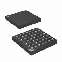
ATXMEGA32A4-CUR Atmel, ATXMEGA32A4-CUR Datasheet - Page 294

ATXMEGA32A4-CUR
Manufacturer Part Number
ATXMEGA32A4-CUR
Description
MCU AVR 32+4 FLASH 49VFBGA
Manufacturer
Atmel
Series
AVR® XMEGAr
Specifications of ATXMEGA32A4-CUR
Core Processor
AVR
Core Size
8/16-Bit
Speed
32MHz
Connectivity
I²C, IrDA, SPI, UART/USART
Peripherals
Brown-out Detect/Reset, DMA, POR, PWM, WDT
Number Of I /o
34
Program Memory Size
32KB (16K x 16)
Program Memory Type
FLASH
Eeprom Size
2K x 8
Ram Size
4K x 8
Voltage - Supply (vcc/vdd)
1.6 V ~ 3.6 V
Data Converters
A/D 12x12b, D/A 2x12b
Oscillator Type
Internal
Operating Temperature
-40°C ~ 85°C
Package / Case
49-VFBGA
For Use With
ATAVRONEKIT - KIT AVR/AVR32 DEBUGGER/PROGRMMRATSTK600 - DEV KIT FOR AVR/AVR32770-1007 - ISP 4PORT ATMEL AVR MCU SPI/JTAG770-1004 - ISP 4PORT FOR ATMEL AVR MCU SPI
Lead Free Status / RoHS Status
Lead free / RoHS Compliant
Available stocks
Company
Part Number
Manufacturer
Quantity
Price
- Current page: 294 of 445
- Download datasheet (6Mb)
25.5
25.6
8077H–AVR–12/09
Voltage reference selection
Conversion Result
As an example of the ADC channel scheme, one of the MUX/result register pairs can be setup to
do single-ended measurements triggered by event signal input, the second MUX/result pair can
measure a differential input on another event signal input, and the two last MUX/result pairs can
measure two other input sources started by the application software.
All the ADC channels use the same ADC for the conversions, but due to the pipelined design a
new conversion can be started on each ADC clock cycle. This means that multiple ADC conver-
sions can be progressing simultaneously and independently without changing the MUX settings.
A conversion result can be kept in one result register, independently of other result registers that
are continuously updated with new conversion results. This can help reduce software complex-
ity, and different software modules can start conversions and read conversion results fully
independent of each other.
The following voltages can be used as the voltage reference (VREF) for the ADC:
•
•
•
•
Figure 25-8. ADC voltage reference selection
The ADC can be set up to be either in signed or in unsigned mode. This setting is global for the
ADC and all ADC channels.
In signed mode, both negative and positive voltages can be measured, both for single ended
and differential input. With 12-bit resolution, the TOP value of a signed result is 2047 and the
results will be in the range -2048 to +2047 (0xF800 - 0x07FF). In unsigned mode the TOP value
is 4095 and results will be in the range 0 - 4095 (0 - 0x0FFF).
Signed mode must be used when any of the ADC inputs are set up for differential measure-
ments. In unsigned mode only single ended or internal signals can be measured.
The result of the analog to digital conversion is written to one of the result registers, RES.
In signed mode the ADC transfer function can be written as:
VINP and VINN are the positive and negative inputs to the ADC. GAIN is 1 unless differential
channels with gain is used.
In unsigned mode the ADC transfer functions can be written as:
Accurate internal 1.00V voltage.
Internal V
External voltage applied to AREF pin on PORTA.
External voltage applied to AREF pin on PORTB.
RES
=
CC
VINP - VINN
-------------------------------- - GAIN TOP
/1.6V voltage.
VREF
⋅
Internal VCC/1.6V
⋅
Internal 1.00V
AREFA
AREFB
VREF
XMEGA A
294
Related parts for ATXMEGA32A4-CUR
Image
Part Number
Description
Manufacturer
Datasheet
Request
R

Part Number:
Description:
DEV KIT FOR AVR/AVR32
Manufacturer:
Atmel
Datasheet:

Part Number:
Description:
INTERVAL AND WIPE/WASH WIPER CONTROL IC WITH DELAY
Manufacturer:
ATMEL Corporation
Datasheet:

Part Number:
Description:
Low-Voltage Voice-Switched IC for Hands-Free Operation
Manufacturer:
ATMEL Corporation
Datasheet:

Part Number:
Description:
MONOLITHIC INTEGRATED FEATUREPHONE CIRCUIT
Manufacturer:
ATMEL Corporation
Datasheet:

Part Number:
Description:
AM-FM Receiver IC U4255BM-M
Manufacturer:
ATMEL Corporation
Datasheet:

Part Number:
Description:
Monolithic Integrated Feature Phone Circuit
Manufacturer:
ATMEL Corporation
Datasheet:

Part Number:
Description:
Multistandard Video-IF and Quasi Parallel Sound Processing
Manufacturer:
ATMEL Corporation
Datasheet:

Part Number:
Description:
High-performance EE PLD
Manufacturer:
ATMEL Corporation
Datasheet:

Part Number:
Description:
8-bit Flash Microcontroller
Manufacturer:
ATMEL Corporation
Datasheet:

Part Number:
Description:
2-Wire Serial EEPROM
Manufacturer:
ATMEL Corporation
Datasheet:


