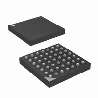
ATXMEGA32A4-CUR Atmel, ATXMEGA32A4-CUR Datasheet - Page 239

ATXMEGA32A4-CUR
Manufacturer Part Number
ATXMEGA32A4-CUR
Description
MCU AVR 32+4 FLASH 49VFBGA
Manufacturer
Atmel
Series
AVR® XMEGAr
Specifications of ATXMEGA32A4-CUR
Core Processor
AVR
Core Size
8/16-Bit
Speed
32MHz
Connectivity
I²C, IrDA, SPI, UART/USART
Peripherals
Brown-out Detect/Reset, DMA, POR, PWM, WDT
Number Of I /o
34
Program Memory Size
32KB (16K x 16)
Program Memory Type
FLASH
Eeprom Size
2K x 8
Ram Size
4K x 8
Voltage - Supply (vcc/vdd)
1.6 V ~ 3.6 V
Data Converters
A/D 12x12b, D/A 2x12b
Oscillator Type
Internal
Operating Temperature
-40°C ~ 85°C
Package / Case
49-VFBGA
For Use With
ATAVRONEKIT - KIT AVR/AVR32 DEBUGGER/PROGRMMRATSTK600 - DEV KIT FOR AVR/AVR32770-1007 - ISP 4PORT ATMEL AVR MCU SPI/JTAG770-1004 - ISP 4PORT FOR ATMEL AVR MCU SPI
Lead Free Status / RoHS Status
Lead free / RoHS Compliant
Available stocks
Company
Part Number
Manufacturer
Quantity
Price
- Current page: 239 of 445
- Download datasheet (6Mb)
21.3.4
21.3.5
8077H–AVR–12/09
Synchronous Clock Operation
SPI Clock Generation
When synchronous mode is used, the XCK pin controls whether the transmission clock is input
(slave mode) or output (master mode). The corresponding port pin must be set to output for
master mode and to input for slave mode. The normal port operation of the XCK pin will be over-
ridden. The dependency between the clock edges and data sampling or data change is the
same. Data input (on RxD) is sampled at the opposite XCK clock edge of the edge where data
output (TxD) is changed.
Figure 21-3. Synchronous Mode XCKn Timing.
Using the Inverted I/O (INVEN) setting in the Pin Configuration Register for the corresponding
XCK port pin, it is selectable which XCK clock edge is used for data sampling and which is used
for data change. If inverted I/O is disabled (INVEN=0) data will be changed at rising XCK clock
edge and sampled at falling XCK clock edge. If inverted I/O is enabled (INVEN=1) data will be
changed at falling XCK clock edge and sampled at rising XCK clock edge. For more details, see
in “I/O Ports” on page 106.
For SPI operation only master mode with internal clock generation is supported. This is identical
to the USART synchronous master mode and the baud rate or BSEL setting are calculated by
using the same equations, see
There are four combinations of the XCK (SCK) clock phase and polarity with respect to serial
data, and these are determined by the Clock Phase (UCPHA) control bit and the Inverted I/O pin
(INVEN) setting. The data transfer timing diagrams are shown in
bits are shifted out and latched in on opposite edges of the XCK signal, ensuring sufficient time
for data signals to stabilize. The UCPHA and INVEN settings are summarized in
page
Receiver and Transmitter.
Table 21-2.
SPI Mode
239. Changing the setting of any of these bits during transmission will corrupt for both the
0
1
2
3
INVEN and UCPHA Functionality
INVEN = 1
INVEN = 0
INVEN
0
0
1
1
RxD / TxD
RxD / TxD
XCK
XCK
Table 21-1 on page
UCPHA
0
1
0
1
Leading Edge
Rising, Sample
Rising, Setup
Falling, Sample
Falling, Setup
238.
Figure 21-4 on page
Sample
Sample
Trailing Edge
Falling, Setup
Falling, Sample
Rising, Setup
Rising, Sample
XMEGA A
Table 21-2 on
240. Data
239
Related parts for ATXMEGA32A4-CUR
Image
Part Number
Description
Manufacturer
Datasheet
Request
R

Part Number:
Description:
DEV KIT FOR AVR/AVR32
Manufacturer:
Atmel
Datasheet:

Part Number:
Description:
INTERVAL AND WIPE/WASH WIPER CONTROL IC WITH DELAY
Manufacturer:
ATMEL Corporation
Datasheet:

Part Number:
Description:
Low-Voltage Voice-Switched IC for Hands-Free Operation
Manufacturer:
ATMEL Corporation
Datasheet:

Part Number:
Description:
MONOLITHIC INTEGRATED FEATUREPHONE CIRCUIT
Manufacturer:
ATMEL Corporation
Datasheet:

Part Number:
Description:
AM-FM Receiver IC U4255BM-M
Manufacturer:
ATMEL Corporation
Datasheet:

Part Number:
Description:
Monolithic Integrated Feature Phone Circuit
Manufacturer:
ATMEL Corporation
Datasheet:

Part Number:
Description:
Multistandard Video-IF and Quasi Parallel Sound Processing
Manufacturer:
ATMEL Corporation
Datasheet:

Part Number:
Description:
High-performance EE PLD
Manufacturer:
ATMEL Corporation
Datasheet:

Part Number:
Description:
8-bit Flash Microcontroller
Manufacturer:
ATMEL Corporation
Datasheet:

Part Number:
Description:
2-Wire Serial EEPROM
Manufacturer:
ATMEL Corporation
Datasheet:


