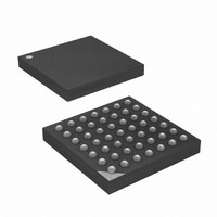
ATXMEGA32A4-CUR Atmel, ATXMEGA32A4-CUR Datasheet - Page 344

ATXMEGA32A4-CUR
Manufacturer Part Number
ATXMEGA32A4-CUR
Description
MCU AVR 32+4 FLASH 49VFBGA
Manufacturer
Atmel
Series
AVR® XMEGAr
Specifications of ATXMEGA32A4-CUR
Core Processor
AVR
Core Size
8/16-Bit
Speed
32MHz
Connectivity
I²C, IrDA, SPI, UART/USART
Peripherals
Brown-out Detect/Reset, DMA, POR, PWM, WDT
Number Of I /o
34
Program Memory Size
32KB (16K x 16)
Program Memory Type
FLASH
Eeprom Size
2K x 8
Ram Size
4K x 8
Voltage - Supply (vcc/vdd)
1.6 V ~ 3.6 V
Data Converters
A/D 12x12b, D/A 2x12b
Oscillator Type
Internal
Operating Temperature
-40°C ~ 85°C
Package / Case
49-VFBGA
For Use With
ATAVRONEKIT - KIT AVR/AVR32 DEBUGGER/PROGRMMRATSTK600 - DEV KIT FOR AVR/AVR32770-1007 - ISP 4PORT ATMEL AVR MCU SPI/JTAG770-1004 - ISP 4PORT FOR ATMEL AVR MCU SPI
Lead Free Status / RoHS Status
Lead free / RoHS Compliant
Available stocks
Company
Part Number
Manufacturer
Quantity
Price
- Current page: 344 of 445
- Download datasheet (6Mb)
29. Program and Debug Interface
29.1
29.2
8077H–AVR–12/09
Features
Overview
•
•
•
•
The Program and Debug Interface (PDI) is an Atmel proprietary interface for external program-
ming and on-chip debugging of the device.
The PDI supports high-speed programming of all Non-Volatile Memory (NVM) spaces; Flash,
EEPOM, Fuses, Lockbits and the User Signature Row. This is done by accessing the NVM Con-
troller, and executing NVM Controller commands as described in Memory Programming.
The On-Chip Debug (OCD) system supports fully intrusive operation. During debugging no soft-
ware or hardware resources in the device is used (except for four I/O pins required if JTAG
connection is used). The OCD system has full program flow control, supports unlimited number
of program and data breakpoints and has full access (read/write) to all memories.
Both programming and debugging can be done through two physical interfaces. The primary
interface is the PDI Physical. This is a 2-pin interface using the Reset pin for the clock input
Program and Debug Interface (PDI)
Programming Features
Debugging Features
JTAG Interface
– 2-pin interface for external programming and on-chip debugging
– Uses Reset pin and dedicated Test pin
– Flexible communication protocol
– 8 Flexible instructions.
– Minimal protocol overhead.
– Fast
– Reliable
– Non-Intrusive Operation
– Complete Program Flow Control
– 1 dedicated program address breakpoint or symbolic breakpoint for AVR studio/emulator
– 4 Hardware Breakpoints
– Unlimited Number of User Program Breakpoints
– Uses CPU for Accessing I/O, Data, and Program
– High Speed Operation
– JTAG (IEEE std. 1149.1 Compliant) Interface
– Boundary-scan Capabilities According to the IEEE std. 1149.1 (JTAG) Standard
– Programming features as for PDI
– On-chip debug features as for PDI
• No I/O pins required during programming or debugging
• 10 MHz programming clock at 1.8V V
• Built in error detection and handling
• Uses no hardware or software resource
• Symbolic Debugging Support in Hardware
• Go, Stop, Reset, Step into, Step over, Step out, Run-to-Cursor
• No limitation on system clock frequency
CC
XMEGA A
344
Related parts for ATXMEGA32A4-CUR
Image
Part Number
Description
Manufacturer
Datasheet
Request
R

Part Number:
Description:
DEV KIT FOR AVR/AVR32
Manufacturer:
Atmel
Datasheet:

Part Number:
Description:
INTERVAL AND WIPE/WASH WIPER CONTROL IC WITH DELAY
Manufacturer:
ATMEL Corporation
Datasheet:

Part Number:
Description:
Low-Voltage Voice-Switched IC for Hands-Free Operation
Manufacturer:
ATMEL Corporation
Datasheet:

Part Number:
Description:
MONOLITHIC INTEGRATED FEATUREPHONE CIRCUIT
Manufacturer:
ATMEL Corporation
Datasheet:

Part Number:
Description:
AM-FM Receiver IC U4255BM-M
Manufacturer:
ATMEL Corporation
Datasheet:

Part Number:
Description:
Monolithic Integrated Feature Phone Circuit
Manufacturer:
ATMEL Corporation
Datasheet:

Part Number:
Description:
Multistandard Video-IF and Quasi Parallel Sound Processing
Manufacturer:
ATMEL Corporation
Datasheet:

Part Number:
Description:
High-performance EE PLD
Manufacturer:
ATMEL Corporation
Datasheet:

Part Number:
Description:
8-bit Flash Microcontroller
Manufacturer:
ATMEL Corporation
Datasheet:

Part Number:
Description:
2-Wire Serial EEPROM
Manufacturer:
ATMEL Corporation
Datasheet:


