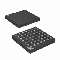
ATXMEGA32A4-CUR Atmel, ATXMEGA32A4-CUR Datasheet - Page 350

ATXMEGA32A4-CUR
Manufacturer Part Number
ATXMEGA32A4-CUR
Description
MCU AVR 32+4 FLASH 49VFBGA
Manufacturer
Atmel
Series
AVR® XMEGAr
Specifications of ATXMEGA32A4-CUR
Core Processor
AVR
Core Size
8/16-Bit
Speed
32MHz
Connectivity
I²C, IrDA, SPI, UART/USART
Peripherals
Brown-out Detect/Reset, DMA, POR, PWM, WDT
Number Of I /o
34
Program Memory Size
32KB (16K x 16)
Program Memory Type
FLASH
Eeprom Size
2K x 8
Ram Size
4K x 8
Voltage - Supply (vcc/vdd)
1.6 V ~ 3.6 V
Data Converters
A/D 12x12b, D/A 2x12b
Oscillator Type
Internal
Operating Temperature
-40°C ~ 85°C
Package / Case
49-VFBGA
For Use With
ATAVRONEKIT - KIT AVR/AVR32 DEBUGGER/PROGRMMRATSTK600 - DEV KIT FOR AVR/AVR32770-1007 - ISP 4PORT ATMEL AVR MCU SPI/JTAG770-1004 - ISP 4PORT FOR ATMEL AVR MCU SPI
Lead Free Status / RoHS Status
Lead free / RoHS Compliant
Available stocks
Company
Part Number
Manufacturer
Quantity
Price
- Current page: 350 of 445
- Download datasheet (6Mb)
29.4
29.4.1
29.4.2
29.4.3
29.4.3.1
8077H–AVR–12/09
JTAG Physical
Enabling
Disabling
JTAG Instruction Set
The PDICOM instruction
Figure 29-9. PDI direction change by inserting IDLE bits
The programmer will loose control of the PDI_DATA line at the point where the PDI target
changes from RX- to TX-mode. The Guard Time relaxes this critical phase of the communica-
tion. When the programmer changes from RX-mode to TX-mode, minimum a single IDLE bit
should be inserted before the start bit is transmitted.
The JTAG physical layer handles the basic low-level serial communication over four I/O lines;
TMS, TCK, TDI, and TDO. The JTAG physical layer includes BREAK detection, parity error
detection, and parity generation. For more details refer to
interface” on page
The JTAGEN Fuse must be programmed and the JTAG Disable bit in the MCU Control Register
must be cleared to enable the JTAG Interface. By default the JTAGEN fuse is programmed, and
the JTAG interface is enabled. When the JTAG instruction PDICOM is shifted into the JTAG
instruction register, the PDI communication register is chosen as the data register connected
between TDI and TDO. In this mode, the JTAG interface can be used to access the PDI for
external programming and on-chip debug.
The JTAG interface can be disabled by either unprogramming the JTAGEN fuse or by setting
the JTAG Disable bit in the MCU Control Register from the application code
The XMEGA JTAG Instruction set consist of eight instructions related to Boundary Scan and PDI
access for NVM programming, for details on the instruction set refer to
page
The 9-bit PDI communication register is selected as data register. Commands are shifted into
the register, while results from previous commands are shifted out from the register. The active
TAP-controller states are:
• Capture-DR: Parallel data from the PDI Controller is sampled into the PDI communication
• Shift-DR: The PDI communication register is shifted by the TCK input.
• Update-DR: Commands or operands are parallel-latched into registers in the PDI Controller.
register.
339.
St
d2W DATA Receive (RX)
337.
1 DATA character
Emulator to d2W
Data from
interface
P
Sp1
Sp2
IDLE bits
Dir. change
Guard time
# IDLE bits
inserted
St
”IEEE 1149.1 JTAG Boundary Scan
d2W DATA Transmit (TX)
1 DATA character
d2W interface
to Emulator
Data from
”JTAG instructions” on
XMEGA A
V
Sp1 Sp2
350
Related parts for ATXMEGA32A4-CUR
Image
Part Number
Description
Manufacturer
Datasheet
Request
R

Part Number:
Description:
DEV KIT FOR AVR/AVR32
Manufacturer:
Atmel
Datasheet:

Part Number:
Description:
INTERVAL AND WIPE/WASH WIPER CONTROL IC WITH DELAY
Manufacturer:
ATMEL Corporation
Datasheet:

Part Number:
Description:
Low-Voltage Voice-Switched IC for Hands-Free Operation
Manufacturer:
ATMEL Corporation
Datasheet:

Part Number:
Description:
MONOLITHIC INTEGRATED FEATUREPHONE CIRCUIT
Manufacturer:
ATMEL Corporation
Datasheet:

Part Number:
Description:
AM-FM Receiver IC U4255BM-M
Manufacturer:
ATMEL Corporation
Datasheet:

Part Number:
Description:
Monolithic Integrated Feature Phone Circuit
Manufacturer:
ATMEL Corporation
Datasheet:

Part Number:
Description:
Multistandard Video-IF and Quasi Parallel Sound Processing
Manufacturer:
ATMEL Corporation
Datasheet:

Part Number:
Description:
High-performance EE PLD
Manufacturer:
ATMEL Corporation
Datasheet:

Part Number:
Description:
8-bit Flash Microcontroller
Manufacturer:
ATMEL Corporation
Datasheet:

Part Number:
Description:
2-Wire Serial EEPROM
Manufacturer:
ATMEL Corporation
Datasheet:


