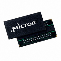
MT47H64M8CB-5E:B Micron Technology Inc, MT47H64M8CB-5E:B Datasheet - Page 87

MT47H64M8CB-5E:B
Manufacturer Part Number
MT47H64M8CB-5E:B
Description
IC DDR2 SDRAM 512MBIT 5NS 60FBGA
Manufacturer
Micron Technology Inc
Datasheet
1.MT47H64M8CB-5EB.pdf
(133 pages)
Specifications of MT47H64M8CB-5E:B
Format - Memory
RAM
Memory Type
DDR2 SDRAM
Memory Size
512M (64M x 8)
Speed
5ns
Interface
Parallel
Voltage - Supply
1.7 V ~ 1.9 V
Operating Temperature
0°C ~ 85°C
Package / Case
60-FBGA
Lead Free Status / RoHS Status
Lead free / RoHS Compliant
Available stocks
Company
Part Number
Manufacturer
Quantity
Price
Company:
Part Number:
MT47H64M8CB-5E:B
Manufacturer:
MICRON
Quantity:
12 388
Company:
Part Number:
MT47H64M8CB-5E:B
Manufacturer:
Micron Technology Inc
Quantity:
10 000
Company:
Part Number:
MT47H64M8CB-5E:B TR
Manufacturer:
Micron Technology Inc
Quantity:
10 000
Table 25:
PDF: 09005aef8117c18e, Source: 09005aef8211b2e6
512MbDDR2_2.fm - Rev. K 8/06 EN
Parameter
Input setup timing measurement reference level
BA1–BA0, A0–A12 A0–A13 (A12 x16), CS#, RAS#, CAS#,
WE#, ODT, DM, UDM, LDM, and CKE
Input hold timing measurement reference level
BA1–BA0, A0–A13 (A12 x16), CS#, RAS#, CAS#, WE#, ODT,
DM, UDM, LDM, and CKE
Input timing measurement reference level (single-ended)
DQS for x4, x8; UDQS, LDQS for x16
Input timing measurement reference level (differential)
CK, CK# for x4, x8, x16
DQS, DQS# for x4, x8; RDQS, RDQS# for x8
UDQS, UDQS#, LDQS, LDQS# for x16
AC Input Test Conditions
Notes:
1. All voltages referenced to V
2. Input waveform setup timing (
3. Input waveform hold (
4. Input waveform setup timing (
5. Input waveform setup timing (
6. Input waveform timing is referenced to the crossing point level (V
7. See “Input Slew Rate Derating” on page 88.
8. The slew rate for single-ended inputs is measured from DC-level to AC-level, (V
9. The slew rate for differentially ended inputs is measured from twice the DC-level to twice
V
test, as shown in Figure 75 on page 102.
level for a rising signal and V
shown in Figure 75 on page 102.
referenced from the crossing of DQS, UDQS, or LDQS through the V
device under test, as shown in Figure 77 on page 103.
enabled is referenced from the cross-point of DQS/DQS#, UDQS/UDQS#, or LDQS/LDQS#, as
shown in Figure 76 on page 102.
(V
is the complementary input signal, as shown in Figure 78 on page 103.
V
to V
Figures 68, 70, 72, and 74.
the AC-level: 2 x V
falling edge). For example, the CK/CK# would be –250mV to +500mV for CK rising edge and
would be +250mV to –500mV for CK falling edge.
IH
IH
TR
(
(
AC
AC
REF
and V
) level for a rising signal and V
) on the rising edge and V
, the valid intersection is where the “tangent” line intersects V
CP
Input Electrical Characteristics and Operating Conditions
) applied to the device under test, where V
IL
(
DC
t
) to 2 x V
IH
b
) timing is referenced from the input signal crossing at the V
SS
87
IH
.
t
(
t
t
Symbol
IS
DS) and hold timing (
DS) and hold timing (
IH
DC
V
IL
REF
b
(
(
V
V
) for a falling signal applied to the device under test, as
AC
V
) is referenced from the input signal crossing at the
AC
RH
RD
RS
(
) on the rising edge and 2 x V
DC
IL
) to V
(
AC
Micron Technology, Inc., reserves the right to change products or specifications without notice.
)
) for a falling signal applied to the device under
IH
(
DC
V
512Mb: x4, x8, x16 DDR2 SDRAM
) on the falling edge. For signals referenced
DD
Min
Q x 0.49
t
t
See Note 2
See Note 3
DH) for single-ended data strobe is
DH) when differential data strobe is
V
TR
IX
(
is the “true” input signal and V
AC
V
)
DD
Max
Q x 0.51
©2004 Micron Technology, Inc. All rights reserved.
IL
IX
(
AC
REF
) of two input signals
REF
) to 2 x V
level applied to the
, as shown in
Units
V
V
IH
IL
(
(
DC
DC
) to
) on the
Notes
1, 2, 7,
1, 3, 7,
1, 4, 7,
1, 5, 6,
7, 9
IL
8
8
8
(
DC
CP
)


