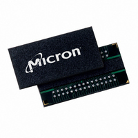
MT47H64M8CB-5E:B Micron Technology Inc, MT47H64M8CB-5E:B Datasheet - Page 128

MT47H64M8CB-5E:B
Manufacturer Part Number
MT47H64M8CB-5E:B
Description
IC DDR2 SDRAM 512MBIT 5NS 60FBGA
Manufacturer
Micron Technology Inc
Datasheet
1.MT47H64M8CB-5EB.pdf
(133 pages)
Specifications of MT47H64M8CB-5E:B
Format - Memory
RAM
Memory Type
DDR2 SDRAM
Memory Size
512M (64M x 8)
Speed
5ns
Interface
Parallel
Voltage - Supply
1.7 V ~ 1.9 V
Operating Temperature
0°C ~ 85°C
Package / Case
60-FBGA
Lead Free Status / RoHS Status
Lead free / RoHS Compliant
Available stocks
Company
Part Number
Manufacturer
Quantity
Price
Company:
Part Number:
MT47H64M8CB-5E:B
Manufacturer:
MICRON
Quantity:
12 388
Company:
Part Number:
MT47H64M8CB-5E:B
Manufacturer:
Micron Technology Inc
Quantity:
10 000
Company:
Part Number:
MT47H64M8CB-5E:B TR
Manufacturer:
Micron Technology Inc
Quantity:
10 000
PDF: 09005aef8117c18e, Source: 09005aef8211b2e6
512MbDDR2_2.fm - Rev. K 8/06 EN
26.
27.
28. No more than four bank-ACTIVE commands may be issued in a given
29.
30. N/A.
31. This is applicable to READ cycles only. WRITE cycles generally require additional time
32.
33. This parameter is not referenced to a specific voltage level, but specified when the
34. When DQS is used single-ended, the minimum limit is reduced by 100ps.
35. The half-clock of
36. The clock’s
37. The inputs to the DRAM must be aligned to the associated clock; that is, the actual
38. Spread spectrum is not included in the jitter specification values. However, the input
39. The period jitter (
40. The half-period jitter (
41. The cycle-to-cycle jitter (
42. The cumulative jitter error (
t
prior to CK, CK# being removed in a system RESET condition. See “Reset Function” on
page 72.
t
Figure 43 on page 62.
period.
8-bank DDR2 devices, regardless of the number of banks already open or closed.
t
the number of banks already open or closed. If a single-bank PRECHARGE command
is issued,
due to
t
tive clock edges. CKE must remain at the valid input level the entire time it takes to
achieve the three clocks of registration. Thus, after any CKE transition, CKE may not
transition from its valid level during the time period of
device output is no longer driving (
value must be derated by the amount of half-clock duty cycle error. For example, if the
clock duty cycle was 47/53,
and 2.5 + 0.03, or 2.53, for
(MIN) is the smallest clock rate allowed, except a deviation due to allowed clock jitter.
Input clock jitter is allowed provided it does not exceed values specified. Also, the jit-
ter must be of a random Gaussian distribution in nature.
clock that latches it in. However, the input timing (in ns) references to the
when determining the required number of clocks. The following input parameters are
determined by taking the specified percentage times the
t
clock can accommodate spread spectrum at a sweep rate in the range 20–60 KHz with
additional one percent of
spread spectrum may not use a clock rate below
age or nominal clock allowed in either the positive or negative direction. JEDEC spec-
ifies tighter jitter numbers during DLL locking time. During DLL lock time, the jitter
values should be 20 percent less than noted in the table (DLL locked).
of clock; however, the two cumulatively can not exceed
cycle to the following cycle. JEDEC specifies tighter jitter numbers during DLL locking
time. During DLL lock time, the jitter values should be 20 percent less than noted in
the table (DLL locked).
amount of clock time allowed to consecutively accumulate away from the average
clock over any number of clock cycles.
DELAY is calculated from
ISXR is equal to
RPA timing applies when the PRECHARGE (ALL) command is issued, regardless of
CKE (MIN) of three clocks means CKE must be registered on three consecutive posi-
DIPW,
t
t
WR during auto precharge.
t
DQSS,
RRD (MIN) restriction still applies. The
t
RP timing applies.
t
CK
AVG
t
DQSH,
t
IS and is used for CKE setup time during self refresh exit, as shown in
t
t
AOFD’s 2.5
JIT
is the average clock over any 200 consecutive clocks and
PER
t
JIT
t
DQSL,
) is the maximum deviation in the clock period from the aver-
t
JIT
t
DTY
t
128
t
CK
AOF (MAX).
IS +
t
t
AOFD would actually be 2.5 - 0.03, or 2.47, for
ERR
CC
) applies to either the high pulse of clock or the low pulse
t
t
AVG
RPA (MIN) applies to all 8-bank DDR2 devices.
CK assumes a 50/50 clock duty cycle. This half-clock
) is the amount the clock period can deviate from one
t
t
DSS,
CK +
nPER
as a long-term jitter component; however, the
t
RPST) or beginning to drive (
Micron Technology, Inc., reserves the right to change products or specifications without notice.
t
), where n is 2, 3, 4, 5, 6–10, or 11–50, is the
t
DSH,
IH so that CKE registration LOW is guaranteed
512Mb: x4, x8, x16 DDR2 SDRAM
t
WPST, and
t
FAW (MIN) parameter applies to all
t
CK
AVG(MIN)
t
t
WPRE.
t
IS + 2 x
JIT
t
CK
PER
©2004 Micron Technology, Inc. All rights reserved.
or above
AVG
.
t
CK +
rather than
t
RPRE).
t
t
CK
IH.
t
FAW (MIN)
AVG(MAX)
t
t
AOF (MIN)
CK
t
t
CK:
CK
AVG
Notes
AVG
.
t
IPW,


