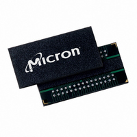
MT47H64M8CB-5E:B Micron Technology Inc, MT47H64M8CB-5E:B Datasheet - Page 40

MT47H64M8CB-5E:B
Manufacturer Part Number
MT47H64M8CB-5E:B
Description
IC DDR2 SDRAM 512MBIT 5NS 60FBGA
Manufacturer
Micron Technology Inc
Datasheet
1.MT47H64M8CB-5EB.pdf
(133 pages)
Specifications of MT47H64M8CB-5E:B
Format - Memory
RAM
Memory Type
DDR2 SDRAM
Memory Size
512M (64M x 8)
Speed
5ns
Interface
Parallel
Voltage - Supply
1.7 V ~ 1.9 V
Operating Temperature
0°C ~ 85°C
Package / Case
60-FBGA
Lead Free Status / RoHS Status
Lead free / RoHS Compliant
Available stocks
Company
Part Number
Manufacturer
Quantity
Price
Company:
Part Number:
MT47H64M8CB-5E:B
Manufacturer:
MICRON
Quantity:
12 388
Company:
Part Number:
MT47H64M8CB-5E:B
Manufacturer:
Micron Technology Inc
Quantity:
10 000
Company:
Part Number:
MT47H64M8CB-5E:B TR
Manufacturer:
Micron Technology Inc
Quantity:
10 000
Figure 20:
Figure 21:
PDF: 09005aef8117c18e, Source: 09005aef8211b2e6
512MbDDR2_2.fm - Rev. K 8/06 EN
COMMAND
DQS, DQS#
ADDRESS
CK#
A10
DQ
CK
VALID 2
READ 1
T0
Nonconsecutive READ Bursts
READ Interrupted by READ
Notes:
Notes:
t CCD
NOP 5
T1
CL = 3 (AL = 0)
COMMAND
COMMAND
COMMAND
1. DO n (or b) = data-out from column n (or column b).
2. BL = 4.
3. Three subsequent elements of data-out appear in the programmed order following DO n.
4. Three subsequent elements of data-out appear in the programmed order following DO b.
5. Shown with nominal
6. Example applies when READ commands are issued to different devices or nonconsecutive
1. BL = 8 required; auto precharge must be disabled (A10 = LOW).
2. READ command can be issued to any valid bank and row address (READ command at T0 and
3. Interrupting READ command must be issued exactly 2 x
4. Auto precharge can be either enabled (A10 = HIGH) or disabled (A10 = LOW) by the inter-
5. NOP or COMMAND INHIBIT commands are valid. PRECHARGE command cannot be issued to
6. Example shown uses AL = 0; CL = 3, BL = 8, shown with nominal
DQS, DQS#
DQS, DQS#
ADDRESS
ADDRESS
ADDRESS
READs.
T2 can be either same bank or different bank).
rupting READ command.
banks used for READs at T0 and T2.
VALID 2
VALID 4
READ 3
CK#
CK#
DQ
DQ
CK
CK
T2
READ
READ
Bank,
Bank,
Col n
Col n
T0
T0
NOP 5
T3
CL = 3 (AL = 0)
D
OUT
CL = 3
NOP
NOP
T1
T1
CL = 4
t
D
AC,
OUT
VALID
T4
t
DQSCK, and
D
NOP
NOP
OUT
T2
T2
40
D
OUT
VALID
T5
READ
READ
Bank,
Bank,
Col b
Col b
T3
T3
Micron Technology, Inc., reserves the right to change products or specifications without notice.
D
t
OUT
DQSQ.
DO
n
T3n
D
DON’T CARE
OUT
512Mb: x4, x8, x16 DDR2 SDRAM
VALID
NOP
NOP
T4
T4
T6
DO
D
n
OUT
T4n
T4n
D
t
OUT
TRANSITIONING DATA
CK from previous READ.
T5
NOP
T5
NOP
VALID
T7
T5n
D
OUT
TRANSITIONING DATA
©2004 Micron Technology, Inc. All rights reserved.
t
AC,
T6
T6
NOP
NOP
D
OUT
DO
t
b
VALID
DQSCK, and
T6n
T8
D
OUT
T7
T7
NOP
NOP
D
DO
b
OUT
T7n
T7n
VALID
T9
t
READs
DON’T CARE
DQSQ.
T8
NOP
T8
NOP


