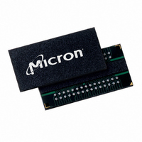
MT47H64M8CB-5E:B Micron Technology Inc, MT47H64M8CB-5E:B Datasheet - Page 63

MT47H64M8CB-5E:B
Manufacturer Part Number
MT47H64M8CB-5E:B
Description
IC DDR2 SDRAM 512MBIT 5NS 60FBGA
Manufacturer
Micron Technology Inc
Datasheet
1.MT47H64M8CB-5EB.pdf
(133 pages)
Specifications of MT47H64M8CB-5E:B
Format - Memory
RAM
Memory Type
DDR2 SDRAM
Memory Size
512M (64M x 8)
Speed
5ns
Interface
Parallel
Voltage - Supply
1.7 V ~ 1.9 V
Operating Temperature
0°C ~ 85°C
Package / Case
60-FBGA
Lead Free Status / RoHS Status
Lead free / RoHS Compliant
Available stocks
Company
Part Number
Manufacturer
Quantity
Price
Company:
Part Number:
MT47H64M8CB-5E:B
Manufacturer:
MICRON
Quantity:
12 388
Company:
Part Number:
MT47H64M8CB-5E:B
Manufacturer:
Micron Technology Inc
Quantity:
10 000
Company:
Part Number:
MT47H64M8CB-5E:B TR
Manufacturer:
Micron Technology Inc
Quantity:
10 000
REFRESH
REFRESH Command
Figure 44:
PDF: 09005aef8117c18e, Source: 09005aef8211b2e6
512MbDDR2_2.fm - Rev. K 8/06 EN
COMMAND
DQS, DQS#
ADDRESS
BANK
A10
DM
CK#
CKE
DQ
CK
1
4
4
4
1
1
NOP
T0
Refresh Mode
2
Notes:
ALL BANKS
ONE BANK
Bank(s)
PRE
T1
REFRESH is used during normal operation of the DDR2 SDRAM and is analogous to
CAS#-Before-RAS# (CBR) REFRESH. This command is nonpersistent, so it must be
issued each time a refresh is required. The addressing is generated by the internal refresh
controller. This makes the address bits a “Don’t Care” during an REFRESH command.
The 512Mb DDR2 SDRAM requires REFRESH cycles at an average interval of 7.8125µs
(MAX). To allow for improved efficiency in scheduling and switching between tasks,
some flexibility in the absolute refresh interval is provided. A maximum of eight
REFRESH commands can be posted (to defer issuing REFRESH commands) to any given
DDR2 SDRAM, meaning that the maximum absolute interval between any REFRESH
command and the next REFRESH command is 9 × 7.8125µs (70.3µs; 3.9µs for high-
temperature operation). The refresh period begins when the REFRESH command is
registered and ends
1. PRE = PRECHARGE, ACT = ACTIVE, AR = REFRESH, RA = row address, BA = bank address.
2. NOP commands are shown for ease of illustration; other valid commands may be possible at
3. “Don’t Care” if A10 is HIGH at this point; A10 must be HIGH if more than one bank is active
4. DM, DQ, and DQS signals are all “Don’t Care”/High-Z for operations shown.
5. The second REFRESH is not required and is only shown as an example of two back-to-back
3
t CK
these times. CKE must be active during clock positive transitions.
(i.e., must precharge all active banks).
REFRESH commands.
NOP
T2
2
t CH
t RP
t CL
NOP
T3
t
RFC (MIN) later.
2
REF
T4
63
t RFC(MIN)
NOP
Micron Technology, Inc., reserves the right to change products or specifications without notice.
Ta0
2
512Mb: x4, x8, x16 DDR2 SDRAM
REF
Ta1
5
Indicates a break in
time scale
NOP
Tb0
©2004 Micron Technology, Inc. All rights reserved.
2
t RFC
NOP
Tb1
5
2
DON’T CARE
REFRESH
Tb2
ACT
BA
RA
RA


