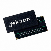
MT47H64M8CB-5E:B Micron Technology Inc, MT47H64M8CB-5E:B Datasheet - Page 14

MT47H64M8CB-5E:B
Manufacturer Part Number
MT47H64M8CB-5E:B
Description
IC DDR2 SDRAM 512MBIT 5NS 60FBGA
Manufacturer
Micron Technology Inc
Datasheet
1.MT47H64M8CB-5EB.pdf
(133 pages)
Specifications of MT47H64M8CB-5E:B
Format - Memory
RAM
Memory Type
DDR2 SDRAM
Memory Size
512M (64M x 8)
Speed
5ns
Interface
Parallel
Voltage - Supply
1.7 V ~ 1.9 V
Operating Temperature
0°C ~ 85°C
Package / Case
60-FBGA
Lead Free Status / RoHS Status
Lead free / RoHS Compliant
Available stocks
Company
Part Number
Manufacturer
Quantity
Price
Company:
Part Number:
MT47H64M8CB-5E:B
Manufacturer:
MICRON
Quantity:
12 388
Company:
Part Number:
MT47H64M8CB-5E:B
Manufacturer:
Micron Technology Inc
Quantity:
10 000
Company:
Part Number:
MT47H64M8CB-5E:B TR
Manufacturer:
Micron Technology Inc
Quantity:
10 000
Functional Description
Figure 4:
PDF: 09005aef8117c18e, Source: 09005aef8211b2e6
512MbDDR2_2.fm - Rev. K 8/06 EN
BA0, BA1
A0–A12,
RAS#
CAS#
ODT
WE#
CKE
CK#
CS#
CK
15
REGISTER
ADDRESS
REGISTERS
MODE
CONTROL
Functional Block Diagram – 32 Meg x 16
LOGIC
15
COUNTER
REFRESH
13
10
2
13
The 512Mb DDR2 SDRAM is a high-speed CMOS dynamic random access memory
containing 536,870,912 bits. The 512Mb DDR2 SDRAM is internally configured as a 4-
bank DRAM.
The 512Mb DDR2 SDRAM uses a double data rate architecture to achieve high-speed
operation. The DDR2 architecture is essentially a 4n-prefetch architecture, with an inter-
face designed to transfer two data words per clock cycle at the I/O balls. A single read or
write access for the 512Mb DDR2 SDRAM consists of a single 4n-bit-wide, one-clock-
cycle data transfer at the internal DRAM core and four corresponding n-bit- wide, one-
half-clock-cycle data transfers at the I/O balls.
Prior to normal operation, the DDR2 SDRAM must be initialized. The following sections
provide detailed information covering device initialization, register definition,
command descriptions, and device operation.
ADDRESS
ROW-
2
MUX
COUNTER/
CONTROL
COLUMN-
ADDRESS
LOGIC
LATCH
13
BANK
ADDRESS
DECODER
LATCH&
BANK 0
ROW-
BANK 1
BANK 2
BANK 3
8
2
8,192
DM MASK LOGIC
SENSE AMPLIFIERS
(8,192 x 128 x 64)
I/O GATING
DECODER
COLUMN
BANK 0
MEMORY
16,384
ARRAY
BANK 1
(x64)
BANK 2
256
BANK 3
Internal
CK, CK#
COL0, COL1
14
64
64
64
LATCH
CK OUT
DRIVERS
READ
WRITE
CK IN
FIFO
&
Micron Technology, Inc., reserves the right to change products or specifications without notice.
16
16
16
16
MASK
DATA
COL0, COL1
64
8
MUX
GENERATOR
512Mb: x4, x8, x16 DDR2 SDRAM
REGISTERS
2
2
2
2
16
16
16
16
DQS
INPUT
DATA
16
16
16
16
16
2
2
2
UDQS, UDQS#
LDQS, LDQS#
2
CK, CK#
16
4
2
DRVRS
DLL
4
RCVRS
Functional Description
©2004 Micron Technology, Inc. All rights reserved.
sw1 sw2
sw1 sw2
sw1 sw2
sw1 sw2
R1
R1
R1
R1
R1
R1
ODT CONTROL
R2
R2
R2
R2
R2
R2
VssQ
sw3
sw3
sw3
sw3
R3
R3
R3
R3
R3
R3
V
DD
Q
DQ0–DQ15
UDQS, UDQS#
LDQS, LDQS#
UDM, LDM


