M30290FAHP#U5A Renesas Electronics America, M30290FAHP#U5A Datasheet - Page 75
M30290FAHP#U5A
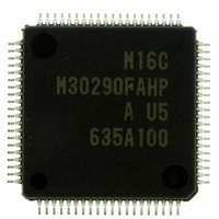
Manufacturer Part Number
M30290FAHP#U5A
Description
IC M16C/29 MCU FLASH 96K 80LQFP
Manufacturer
Renesas Electronics America
Series
M16C™ M16C/Tiny/29r
Datasheet
1.M30291FCHPU5A.pdf
(501 pages)
Specifications of M30290FAHP#U5A
Core Processor
M16C/60
Core Size
16-Bit
Speed
20MHz
Connectivity
CAN, I²C, IEBus, SIO, UART/USART
Peripherals
DMA, POR, PWM, Voltage Detect, WDT
Number Of I /o
71
Program Memory Size
96KB (96K x 8)
Program Memory Type
FLASH
Ram Size
8K x 8
Voltage - Supply (vcc/vdd)
2.7 V ~ 5.5 V
Data Converters
A/D 27x10b
Oscillator Type
Internal
Operating Temperature
-20°C ~ 85°C
Package / Case
80-LQFP
For Use With
R0K330290S000BE - KIT EVAL STARTER FOR M16C/29M30290T2-CPE - EMULATOR COMPACT M16C/26A/28/29M30290T2-CPE-HP - EMULATOR COMPACT FOR M16C/TINY
Lead Free Status / RoHS Status
Lead free / RoHS Compliant
Eeprom Size
-
Available stocks
Company
Part Number
Manufacturer
Quantity
Price

Part Number:
M30290FAHP#U5AM30290FAHP#D3
Manufacturer:
Renesas Electronics America
Quantity:
10 000
Part Number:
M30290FAHP#U5AM30290FAHP#U3A
Manufacturer:
Renesas Electronics America
Quantity:
135
Part Number:
M30290FAHP#U5AM30290FAHP#U3A
Manufacturer:
Renesas Electronics America
Quantity:
10 000


R
R
M
e
E
1
. v
J
Figure 7.2 CM0 Register
6
0
1
C
9
1 .
B
2 /
NOTES:
b7
System Clock Control Register 0
0
2
10. When the PM21 bit in the PM2 register is set to 1 (clock modification disable), writing to bits CM02, CM05, and CM07 has
11. If the PM21 bit needs to be set to 1, set the CM07 bit to 0 (main clock) before setting it.
12. To use the main clock a the clock source for the CPU clock, follow the procedure below.
13. When the CM21 bit is set to 0 (on-chip oscillaor turned off) and the CM05 bit is set to 1 (main clock turned off), the CM06 bit
14. To return from on-chip oscillator mode to high-speed or middle-speed mode set both bits CM06 and CM15 to 1.
9
1
1. Write to this register after setting the PRC0 bit in the PRCR register to 1 (write enable).
2. The CM03 bit is set to 1 (high) when the CM04 bit is set to 0 (I/O port) or the MCU goes to a stop mode.
3. This bit is provided to stop the main clock when the low power dissipation mode or on-chip oscillator low power dissipation mode
4. During external clock input, set the CM05 bit to 0 (On).
5. When CM05 bit is set to 1, the X
6. After setting the CM04 bit to 1 (X
7. When entering stop mode from high or middle speed mode, on-chip oscillator mode or on-chip oscillator low power mode, the
8. The f
9. To use a sub-clock, set this bit to 1. Also, make sure ports P8
M
0
b6
G
is selected. This bit cannot be used for detection as to whether the main clock stopped or not. To stop the main clock, the
following setting is required:
(1) Set the CM07 bit to 1 (Sub-clock select) or the CM21 bit in the CM2 register to 1 (on-chip oscillator select) with the sub-
(2) Set the CM20 bit in the CM2 register to 0 (Oscillation stop, re-oscillation detection function disabled).
(3) Set the CM05 bit to 1 (Stop).
the X
the CM07 bit from 0 to 1 (sub-clock).
CM06 bit is set to 1 (divided-by-8 mode).
off in wait mode).
no effect.
(1) Set the CM05 bit to 0 (oscillate).
(2) Wait the main clock oscillation stabilized.
(3) Set all bits CM11, CM21, and CM07 to 0.
is fixed to 1 (divide-by-8 mode) and the CM15 bit is fixed to 1 (drive capability High).
1
r a
0 -
o r
b5
3 .
clock stably oscillating.
1
u
C32
, 0
IN
b4
1
p
2
pin is pulled "H" to the same level as X
2
clock does not stop. During low speed or low power dissipation mode, do not set this bit to 1(peripheral clock turned
b3
0
0
b2
7
b1
b0
page 49
Bit Symbol
CM00
CM01
CM02
CM03
CM04
CM05
CM06
CM07
Symbol
CM0
OUT
f o
CIN
-X
4
pin goes "H". Futhermore, because the internal feedback resistor remains connectes,
5
Port X
Main clock division select
bit 0
COUT
Clock output function
select bit
Wait Mode peripheral function
clock stop bit
X
select bit
Main clock stop bit
(3, 10, 12, 13)
System clock select bit
(6, 10, 11, 12)
8
(1)
CIN
-X
(7, 13, 14)
oscillator function), wait until the sub-clock oscillates stably before switching
C
COUT
OUT
select bit
Bit Name
(2)
via the feedback resistor.
Address
0006
drive capacity
(10)
(2)
16
6
and P8
See Table 7.3
0: Do not stop peripheral function clock in wait mode
1: Stop peripheral function clock in wait mode
0: LOW
1: HIGH
0: I/O port P8
1: X
0: On
1: Off
0: CM16 and CM17 valid
1: Division by 8 mode
0: Main clock, PLL clock, or on-chip oscillator clock
1: Sub-clock
7
After Reset
01001000
CIN
are directed for input, with no pull-ups.
(4)
(5)
-X
COUT
6
2
generation function
, P8
7
Function
(9)
(8)
RW
RW
RW
RW
RW
RW
RW
RW
RW
Related parts for M30290FAHP#U5A
Image
Part Number
Description
Manufacturer
Datasheet
Request
R

Part Number:
Description:
KIT STARTER FOR M16C/29
Manufacturer:
Renesas Electronics America
Datasheet:

Part Number:
Description:
KIT STARTER FOR R8C/2D
Manufacturer:
Renesas Electronics America
Datasheet:

Part Number:
Description:
R0K33062P STARTER KIT
Manufacturer:
Renesas Electronics America
Datasheet:

Part Number:
Description:
KIT STARTER FOR R8C/23 E8A
Manufacturer:
Renesas Electronics America
Datasheet:

Part Number:
Description:
KIT STARTER FOR R8C/25
Manufacturer:
Renesas Electronics America
Datasheet:

Part Number:
Description:
KIT STARTER H8S2456 SHARPE DSPLY
Manufacturer:
Renesas Electronics America
Datasheet:

Part Number:
Description:
KIT STARTER FOR R8C38C
Manufacturer:
Renesas Electronics America
Datasheet:

Part Number:
Description:
KIT STARTER FOR R8C35C
Manufacturer:
Renesas Electronics America
Datasheet:

Part Number:
Description:
KIT STARTER FOR R8CL3AC+LCD APPS
Manufacturer:
Renesas Electronics America
Datasheet:
Part Number:
Description:
KIT STARTER FOR RX610
Manufacturer:
Renesas Electronics America
Datasheet:

Part Number:
Description:
KIT STARTER FOR R32C/118
Manufacturer:
Renesas Electronics America
Datasheet:

Part Number:
Description:
KIT DEV RSK-R8C/26-29
Manufacturer:
Renesas Electronics America
Datasheet:

Part Number:
Description:
KIT STARTER FOR SH7124
Manufacturer:
Renesas Electronics America
Datasheet:

Part Number:
Description:
KIT STARTER FOR H8SX/1622
Manufacturer:
Renesas Electronics America
Datasheet:

Part Number:
Description:
KIT DEV FOR SH7203
Manufacturer:
Renesas Electronics America
Datasheet: