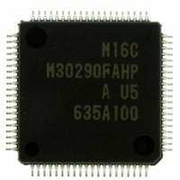
M30290FAHP#U5A Renesas Electronics America, M30290FAHP#U5A Datasheet - Page 248

M30290FAHP#U5A
Manufacturer Part Number
M30290FAHP#U5A
Description
IC M16C/29 MCU FLASH 96K 80LQFP
Manufacturer
Renesas Electronics America
Series
M16C™ M16C/Tiny/29r
Datasheet
1.M30291FCHPU5A.pdf
(501 pages)
Specifications of M30290FAHP#U5A
Core Processor
M16C/60
Core Size
16-Bit
Speed
20MHz
Connectivity
CAN, I²C, IEBus, SIO, UART/USART
Peripherals
DMA, POR, PWM, Voltage Detect, WDT
Number Of I /o
71
Program Memory Size
96KB (96K x 8)
Program Memory Type
FLASH
Ram Size
8K x 8
Voltage - Supply (vcc/vdd)
2.7 V ~ 5.5 V
Data Converters
A/D 27x10b
Oscillator Type
Internal
Operating Temperature
-20°C ~ 85°C
Package / Case
80-LQFP
For Use With
R0K330290S000BE - KIT EVAL STARTER FOR M16C/29M30290T2-CPE - EMULATOR COMPACT M16C/26A/28/29M30290T2-CPE-HP - EMULATOR COMPACT FOR M16C/TINY
Lead Free Status / RoHS Status
Lead free / RoHS Compliant
Eeprom Size
-
Available stocks
Company
Part Number
Manufacturer
Quantity
Price
Part Number:
M30290FAHP#U5AM30290FAHP#D3
Manufacturer:
Renesas Electronics America
Quantity:
10 000
Part Number:
M30290FAHP#U5AM30290FAHP#U3A
Manufacturer:
Renesas Electronics America
Quantity:
135
Part Number:
M30290FAHP#U5AM30290FAHP#U3A
Manufacturer:
Renesas Electronics America
Quantity:
10 000
- Current page: 248 of 501
- Download datasheet (5Mb)
R
R
15. A/D Converter
e
E
. v
J
NOTES:
Table 15.1 A/D Converter Performance
0
The MCU contains one A/D converter circuit based on 10-bit successive approximation method configured
with a capacitive-coupling amplifier. The analog inputs share the pins with P10
to P0
Similarly, AD
sponding port direction bits are set to 0 (input mode).
When not using the A/D converter, set the VCUT bit to 0 (Vref unconnected), so that no current will flow
from the Vref pin into the resistor ladder, helping to reduce the power consumption of the chip.
The A/D conversion result is stored in the ADi register bits for AN
= 0 to 2). Table 15.1 shows the A/D converter performance. Figure 15.1 shows the A/D converter block
diagram and Figures 15.2 to 15.4 show the A/D converter associated with registers.
A/D Conversion Method
Analog Input Voltage
Operating Clock
Resolution
Integral Nonlinearity Error When AV
Operating Modes
Analog Input Pins
Conversion Speed Per Pin
1
9
1 .
B
1. Not dependent on use of sample and hold function.
2. Set the AD frequency to 10 MHz or less.
0
2
Ports P0
available in 64-pin package. Do not use port P0
and P9
Note
With the sample and hold function, set the AD frequency to 1MH
1
Without sample-and-hold function, set the AD frequency to 250kH
M
7
0
1
r a
(AN0
0 -
3 .
Item
1
____________
, 0
5
1
2
4
to P9
0
2
TRG
to P0
0
to AN0
0
7
AD
7
input shares the pin with P1
(AN2
7
(2)
(1)
(AN0
page 222
7
), and P1
5
4
to AN2
to AN0
Successive approximation (capacitive coupling amplifier)
0V to AV
f
or f
8-bit or 10-bit (selectable)
• With 8-bit resolution: 2LSB
• With 10-bit resolution: 3LSB
When AV
• With 8-bit resolution: 2LSB
• With 10-bit resolution: 5LSB
One-shot mode, repeat mode, single sweep mode, repeat sweep mode 0, repeat
sweep mode 1, simultaneous sample sweep mode and delayed trigger mode 0,1
8 pins (AN
to AN3
8 pins (AN
• Without sample and hold function
• With sample and hold function
AD
(64-pin package)
8-bit resolution: 49
8-bit resolution: 28
f o
/divided-by-2 or f
AD
0
7
4
to P1
) as analog input pins in 64-pin package.
5
/divided-by-12 or f
7
2
8
), P1
)
CC
0
0
CC
CC
3
(80-pin package)
to AN
to AN
, P9
0
(V
= Vref = 5V
= Vref = 3.3V
to P1
CC
3
7
7
, P9
)
) + 8 pins (AN0
) + 4 pins (AN0
5
. Therefore, when using these inputs, make sure the corre-
3
(AN2
AD
5
AD
AD
to P9
/divided-by-3 or f
4
AD
cycles, 10-bit resolution: 59
cycles, 10-bit resolution: 33
0
to P0
to AN2
7
(AN2
7
0
0
(AN0
Performance
to AN0
to AN0
3
0
) and P9
Z
to AN2
4
Z
or more.
i
, AN0
7
3
to AN0
or more.
) + 8 pins (AN2
) + 1 pin (AN2
AD
/divided-by-4 or f
7
5
i
), and P9
, AN2
to P9
7
), P1
i
7
0
(i = 0 to 7), and AN3
0
(AN2
to P10
4
to P1
) + 3 pins (AN3
0
0
AD
AD
to AN2
to P9
5
cycles
cycles
to AN2
3
7
AD
(AN2
(AN
2
7
/divided-by-6
(AN3
) + 3 pins (AN3
0
0
7
to AN
to AN2
) are not
0
0
to AN3
to AN3
i
7
pins (i
), P0
3
)
2
)
0
2
).
0
Related parts for M30290FAHP#U5A
Image
Part Number
Description
Manufacturer
Datasheet
Request
R

Part Number:
Description:
KIT STARTER FOR M16C/29
Manufacturer:
Renesas Electronics America
Datasheet:

Part Number:
Description:
KIT STARTER FOR R8C/2D
Manufacturer:
Renesas Electronics America
Datasheet:

Part Number:
Description:
R0K33062P STARTER KIT
Manufacturer:
Renesas Electronics America
Datasheet:

Part Number:
Description:
KIT STARTER FOR R8C/23 E8A
Manufacturer:
Renesas Electronics America
Datasheet:

Part Number:
Description:
KIT STARTER FOR R8C/25
Manufacturer:
Renesas Electronics America
Datasheet:

Part Number:
Description:
KIT STARTER H8S2456 SHARPE DSPLY
Manufacturer:
Renesas Electronics America
Datasheet:

Part Number:
Description:
KIT STARTER FOR R8C38C
Manufacturer:
Renesas Electronics America
Datasheet:

Part Number:
Description:
KIT STARTER FOR R8C35C
Manufacturer:
Renesas Electronics America
Datasheet:

Part Number:
Description:
KIT STARTER FOR R8CL3AC+LCD APPS
Manufacturer:
Renesas Electronics America
Datasheet:

Part Number:
Description:
KIT STARTER FOR RX610
Manufacturer:
Renesas Electronics America
Datasheet:

Part Number:
Description:
KIT STARTER FOR R32C/118
Manufacturer:
Renesas Electronics America
Datasheet:

Part Number:
Description:
KIT DEV RSK-R8C/26-29
Manufacturer:
Renesas Electronics America
Datasheet:

Part Number:
Description:
KIT STARTER FOR SH7124
Manufacturer:
Renesas Electronics America
Datasheet:

Part Number:
Description:
KIT STARTER FOR H8SX/1622
Manufacturer:
Renesas Electronics America
Datasheet:

Part Number:
Description:
KIT DEV FOR SH7203
Manufacturer:
Renesas Electronics America
Datasheet:


