M30290FAHP#U5A Renesas Electronics America, M30290FAHP#U5A Datasheet - Page 245
M30290FAHP#U5A
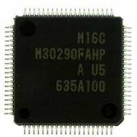
Manufacturer Part Number
M30290FAHP#U5A
Description
IC M16C/29 MCU FLASH 96K 80LQFP
Manufacturer
Renesas Electronics America
Series
M16C™ M16C/Tiny/29r
Datasheet
1.M30291FCHPU5A.pdf
(501 pages)
Specifications of M30290FAHP#U5A
Core Processor
M16C/60
Core Size
16-Bit
Speed
20MHz
Connectivity
CAN, I²C, IEBus, SIO, UART/USART
Peripherals
DMA, POR, PWM, Voltage Detect, WDT
Number Of I /o
71
Program Memory Size
96KB (96K x 8)
Program Memory Type
FLASH
Ram Size
8K x 8
Voltage - Supply (vcc/vdd)
2.7 V ~ 5.5 V
Data Converters
A/D 27x10b
Oscillator Type
Internal
Operating Temperature
-20°C ~ 85°C
Package / Case
80-LQFP
For Use With
R0K330290S000BE - KIT EVAL STARTER FOR M16C/29M30290T2-CPE - EMULATOR COMPACT M16C/26A/28/29M30290T2-CPE-HP - EMULATOR COMPACT FOR M16C/TINY
Lead Free Status / RoHS Status
Lead free / RoHS Compliant
Eeprom Size
-
Available stocks
Company
Part Number
Manufacturer
Quantity
Price

Part Number:
M30290FAHP#U5AM30290FAHP#D3
Manufacturer:
Renesas Electronics America
Quantity:
10 000
Part Number:
M30290FAHP#U5AM30290FAHP#U3A
Manufacturer:
Renesas Electronics America
Quantity:
135
Part Number:
M30290FAHP#U5AM30290FAHP#U3A
Manufacturer:
Renesas Electronics America
Quantity:
10 000


R
R
M
e
E
1
. v
J
Table 14.20 SI/O3 and SI/O4 Specifications
NOTE:
6
0
Interrupt request
generation timing
1
C
Transfer data format
Transfer clock
Transmission/reception
start condition
CLKi pin fucntion
S
SINi pin function
Select function
9
1 .
B
OUT
2 /
1. To set the SMi6 bit in the SiC register to 0 (external clock), follow the procedure described below.
3. When the SMi6 bit in the SiC register is set to 1 (internal clock), S
4. When the SMi6 bit in the SiC register is set to 1 (internal clock), the transfer clock stops in the high state if the
0
2
9
1
• If the SMi4 bit in the SiC register is set to 0, write transmit data to the SiTRR register while input on the CLKi
• If the SMi4 bit is set to 1, write transmit data to the SiTRR register while input on the CLKi pin is low. The same
• Because shift operation continues as long as the transfer clock is supplied to the SI/Oi circuit, stop the transfer
clock period after completion of transfer and, thereafter, goes to a high-impedance state. However, if transmit
data is written to the SiTRR register during this period, S
the data hold time thereby reduced.
SMi4 bit is set to 0, or stops in the low state if the SMi4 bit is set to 1.
M
i pin function
0
pin is high. The same applies when rewriting the SMi7 bit in the SiC register.
applies when rewriting the SMi7 bit.
clock 2. Unlike UART0 to UART2, SI/Oi (i = 3 to 4) is not separated between the transfer register and buffer.
Therefore, do not write the next transmit data to the SiTRR register during transmission.
G
1
r a
0 -
o r
3 .
1
u
Item
, 0
1
p
2
2
0
0
7
page 219
• Transfer data length: 8 bits
• The SMi6 bit in the SiC (i=3, 4) register is set to 1 (internal clock) : fj/ (2(n+1))
• SMi6 bit is set to 0 (external clock) : Input from CLKi pin
• Before transmission/reception can start, the following requirements must be met
• When the SMi4 bit in the SiC register is set to 0
• When SMi4 is set to 1
I/O port, transfer clock input, transfer clock output
I/O port, transmit data output, high-impedance
I/O port, receive data input
• LSB first or MSB first selection
• Function for setting an S
• CLK polarity selection
fj = f
Write transmit data to the SiTRR register
The rising edge of the last transfer clock pulse
The falling edge of the last transfer clock pulse
Whether to start sending/receiving data beginning with bit 0 or beginning with bit 7
can be selected
When the SMi6 bit in the SiC register is set to 0 (external clock), the S
output level while not tranmitting can be selected.
Whether transmit data is output/input timing at the rising edge or falling edge of
transfer clock can be selected.
f o
4
1SIO
5
8
, f
2SIO
, f
8SIO
, f
32SIO
OUT
. n=Setting value of SiBRG register
OUTi
i initial value set function
immediately goes to a high-impedance state, with
Specification
OUTi
(2, 3)
retains the last data for a 1/2 transfer
(4)
(4)
(1)
00
16
OUT
to FF
i pin
16
.
Related parts for M30290FAHP#U5A
Image
Part Number
Description
Manufacturer
Datasheet
Request
R

Part Number:
Description:
KIT STARTER FOR M16C/29
Manufacturer:
Renesas Electronics America
Datasheet:

Part Number:
Description:
KIT STARTER FOR R8C/2D
Manufacturer:
Renesas Electronics America
Datasheet:

Part Number:
Description:
R0K33062P STARTER KIT
Manufacturer:
Renesas Electronics America
Datasheet:

Part Number:
Description:
KIT STARTER FOR R8C/23 E8A
Manufacturer:
Renesas Electronics America
Datasheet:

Part Number:
Description:
KIT STARTER FOR R8C/25
Manufacturer:
Renesas Electronics America
Datasheet:

Part Number:
Description:
KIT STARTER H8S2456 SHARPE DSPLY
Manufacturer:
Renesas Electronics America
Datasheet:

Part Number:
Description:
KIT STARTER FOR R8C38C
Manufacturer:
Renesas Electronics America
Datasheet:

Part Number:
Description:
KIT STARTER FOR R8C35C
Manufacturer:
Renesas Electronics America
Datasheet:

Part Number:
Description:
KIT STARTER FOR R8CL3AC+LCD APPS
Manufacturer:
Renesas Electronics America
Datasheet:
Part Number:
Description:
KIT STARTER FOR RX610
Manufacturer:
Renesas Electronics America
Datasheet:

Part Number:
Description:
KIT STARTER FOR R32C/118
Manufacturer:
Renesas Electronics America
Datasheet:

Part Number:
Description:
KIT DEV RSK-R8C/26-29
Manufacturer:
Renesas Electronics America
Datasheet:

Part Number:
Description:
KIT STARTER FOR SH7124
Manufacturer:
Renesas Electronics America
Datasheet:

Part Number:
Description:
KIT STARTER FOR H8SX/1622
Manufacturer:
Renesas Electronics America
Datasheet:

Part Number:
Description:
KIT DEV FOR SH7203
Manufacturer:
Renesas Electronics America
Datasheet: