M30290FAHP#U5A Renesas Electronics America, M30290FAHP#U5A Datasheet - Page 172
M30290FAHP#U5A
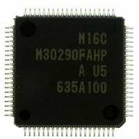
Manufacturer Part Number
M30290FAHP#U5A
Description
IC M16C/29 MCU FLASH 96K 80LQFP
Manufacturer
Renesas Electronics America
Series
M16C™ M16C/Tiny/29r
Datasheet
1.M30291FCHPU5A.pdf
(501 pages)
Specifications of M30290FAHP#U5A
Core Processor
M16C/60
Core Size
16-Bit
Speed
20MHz
Connectivity
CAN, I²C, IEBus, SIO, UART/USART
Peripherals
DMA, POR, PWM, Voltage Detect, WDT
Number Of I /o
71
Program Memory Size
96KB (96K x 8)
Program Memory Type
FLASH
Ram Size
8K x 8
Voltage - Supply (vcc/vdd)
2.7 V ~ 5.5 V
Data Converters
A/D 27x10b
Oscillator Type
Internal
Operating Temperature
-20°C ~ 85°C
Package / Case
80-LQFP
For Use With
R0K330290S000BE - KIT EVAL STARTER FOR M16C/29M30290T2-CPE - EMULATOR COMPACT M16C/26A/28/29M30290T2-CPE-HP - EMULATOR COMPACT FOR M16C/TINY
Lead Free Status / RoHS Status
Lead free / RoHS Compliant
Eeprom Size
-
Available stocks
Company
Part Number
Manufacturer
Quantity
Price

Part Number:
M30290FAHP#U5AM30290FAHP#D3
Manufacturer:
Renesas Electronics America
Quantity:
10 000
Part Number:
M30290FAHP#U5AM30290FAHP#U3A
Manufacturer:
Renesas Electronics America
Quantity:
135
Part Number:
M30290FAHP#U5AM30290FAHP#U3A
Manufacturer:
Renesas Electronics America
Quantity:
10 000


R
R
e
E
. v
J
Figure 13.6 G1TM0 to G1TM7 Registers, and G1POCR0 to G1POCR7 Registers
0
1
9
1 .
B
0
2
1
M
0
(b7)
b15
Waveform Generation Register j (j=0 to 7)
1
r a
Waveform Generation Control Register j (j=0 to 7)
0 -
b7
3 .
NOTES :
1
, 0
1
b6
1. This setting is enabled only for even channels. In SR waveform output mode, values written to the
2. The inverse output function is the final step in waveform generating process. When the INV bit is set
3. In the SR waveform output mode, set not only the even channel but also the correspoinding even
4. To provide either "H" or "L" signal output set in the IVL bit, set the FSCj bit in the G1FS register to 0
2
2
corresponding odd channel (next channel after an even channel) are ignored. Even channels
provide waveform output. Odd channels provide no waveform output.
to 1, and "H" signal is provided a default output by setting the IVL bit to 0, and an "L" signal is
provided by setting it to 1.
channel (next channel after the even channel).
(select waveform generating function) and IFEj bit in the G1FE register to 1 (functions for channel j
enabled). Then set the IVL bit to 0 or 1.
b5
0
0
(b0)
b8
7
b4
b7
b3
page 146
b2
b1
b0
b0
f o
(b3-b2)
The base timer value is stored every
measurement timing
Symbol
MOD0
MOD1
4
RLD
(b6)
Symbol
G1TM0 to G1TM2
G1TM3 to G1TM5
G1TM6 to G1TM7
INV
5
IVL
Bit
8
Symbol
G1POCR0 to G1POCR3
G1POCR4 to G1POCR7
Operating mode
select bit
Nothing is assigned. If necessary, set to 0.
When read, their contents are undefined
Output initial value
select bit
G1POj register value
reload timing select bit
Inverse output function
select bit
Nothing is assigned. If necessary, set to 0.
When read, its content is undefined
Function
Bit Name
(4)
(2)
0301
0307
030D
Address
16
16
16
-0300
-0306
-030C
16,
16,
Address
0310
0314
16,
0303
0309
030F
b1
0: "L" output as a default value
1: "H" output as a default value
0: Reloads the G1POj register when
1: Reloads the G1POj register when
0: Output is not inversed
1: Output is inversed
0
0
1
1
16
16
b0
0
1
0
1
, 0311
, 0315
value is written
the base timer is reset
: Single waveform output mode
: SR waveform output mode
: Phase-delayed waveform
: Do not set to this value
16
16
16
output mode
-0302
-0308
-030E
16
16
, 0312
, 0316
16,
16,
16
0305
030B
Function
16
16
, 0313
, 0317
Setting Range
16
16
-0304
-030A
16
16
16
16
After Reset
Indeterminte
Indeterminte
Indeterminte
After Reset
0X00 XX00
0X00 XX00
(1)
RW
RO
RW
RW
RW
RW
RW
RW
2
2
Related parts for M30290FAHP#U5A
Image
Part Number
Description
Manufacturer
Datasheet
Request
R

Part Number:
Description:
KIT STARTER FOR M16C/29
Manufacturer:
Renesas Electronics America
Datasheet:

Part Number:
Description:
KIT STARTER FOR R8C/2D
Manufacturer:
Renesas Electronics America
Datasheet:

Part Number:
Description:
R0K33062P STARTER KIT
Manufacturer:
Renesas Electronics America
Datasheet:

Part Number:
Description:
KIT STARTER FOR R8C/23 E8A
Manufacturer:
Renesas Electronics America
Datasheet:

Part Number:
Description:
KIT STARTER FOR R8C/25
Manufacturer:
Renesas Electronics America
Datasheet:

Part Number:
Description:
KIT STARTER H8S2456 SHARPE DSPLY
Manufacturer:
Renesas Electronics America
Datasheet:

Part Number:
Description:
KIT STARTER FOR R8C38C
Manufacturer:
Renesas Electronics America
Datasheet:

Part Number:
Description:
KIT STARTER FOR R8C35C
Manufacturer:
Renesas Electronics America
Datasheet:

Part Number:
Description:
KIT STARTER FOR R8CL3AC+LCD APPS
Manufacturer:
Renesas Electronics America
Datasheet:
Part Number:
Description:
KIT STARTER FOR RX610
Manufacturer:
Renesas Electronics America
Datasheet:

Part Number:
Description:
KIT STARTER FOR R32C/118
Manufacturer:
Renesas Electronics America
Datasheet:

Part Number:
Description:
KIT DEV RSK-R8C/26-29
Manufacturer:
Renesas Electronics America
Datasheet:

Part Number:
Description:
KIT STARTER FOR SH7124
Manufacturer:
Renesas Electronics America
Datasheet:

Part Number:
Description:
KIT STARTER FOR H8SX/1622
Manufacturer:
Renesas Electronics America
Datasheet:

Part Number:
Description:
KIT DEV FOR SH7203
Manufacturer:
Renesas Electronics America
Datasheet: