M30290FAHP#U5A Renesas Electronics America, M30290FAHP#U5A Datasheet - Page 273
M30290FAHP#U5A
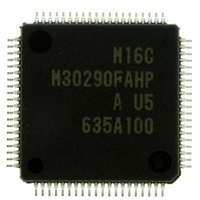
Manufacturer Part Number
M30290FAHP#U5A
Description
IC M16C/29 MCU FLASH 96K 80LQFP
Manufacturer
Renesas Electronics America
Series
M16C™ M16C/Tiny/29r
Datasheet
1.M30291FCHPU5A.pdf
(501 pages)
Specifications of M30290FAHP#U5A
Core Processor
M16C/60
Core Size
16-Bit
Speed
20MHz
Connectivity
CAN, I²C, IEBus, SIO, UART/USART
Peripherals
DMA, POR, PWM, Voltage Detect, WDT
Number Of I /o
71
Program Memory Size
96KB (96K x 8)
Program Memory Type
FLASH
Ram Size
8K x 8
Voltage - Supply (vcc/vdd)
2.7 V ~ 5.5 V
Data Converters
A/D 27x10b
Oscillator Type
Internal
Operating Temperature
-20°C ~ 85°C
Package / Case
80-LQFP
For Use With
R0K330290S000BE - KIT EVAL STARTER FOR M16C/29M30290T2-CPE - EMULATOR COMPACT M16C/26A/28/29M30290T2-CPE-HP - EMULATOR COMPACT FOR M16C/TINY
Lead Free Status / RoHS Status
Lead free / RoHS Compliant
Eeprom Size
-
Available stocks
Company
Part Number
Manufacturer
Quantity
Price

Part Number:
M30290FAHP#U5AM30290FAHP#D3
Manufacturer:
Renesas Electronics America
Quantity:
10 000
Part Number:
M30290FAHP#U5AM30290FAHP#U3A
Manufacturer:
Renesas Electronics America
Quantity:
135
Part Number:
M30290FAHP#U5AM30290FAHP#U3A
Manufacturer:
Renesas Electronics America
Quantity:
10 000


R
R
M
e
E
1
. v
J
NOTES:
Table 15.12 Delayed Trigger Mode 1 Specifications
6
0
A/D Conversion Start
Readout of A/D Conversion Result
Function
Condition
A/D Conversion Stop
Condition
Interrupt Request
Generation Timing
Analog Input Pin
15.1.8 Delayed Trigger Mode 1
1
9
C
1 .
B
In delayed trigger mode 1, analog voltages applied to the selected pins are converted one-by-one to a
digital code. When the input of the AD
conversion is started. After completing the AN
until the second AD
the single sweep conversion of the pins after the AN
trigger mode 1 specifications. Figure 15.24 shows the operation example of delayed trigger mode 1.
Figure 15.25 and 15.26 show each flag operation in the ADSTAT0 register that corresponds to the
operation example. Figure 15.27 shows registers ADCON0 to ADCON2 in delayed trigger mode 1.
Figure 15.28 shows the ADTRGCON register in delayed trigger mode 1. Table 15.13 shows the trigger
select bit setting in delayed trigger mode 1.
1. Do not generate the next AD
2. The AD
3. Do not write 1 (A/D conversion started) to the ADST bit in delayed trigger mode 1. When write 1,unexpected
4. AN0
2 /
0
2
9
1
complete A/D conversion. When an AD
is ignored. The falling edge of AD
considered to be the next AN0 pin conversion start condition.
falling edge is generated in shorter periods than fAD, the second AD
not generate the AD
interrupts may be generated.
pins need to belong to the same group.
M
0
G
1
Item
r a
0 -
o r
___________
0
3 .
1
to AN0
u
, 0
1
p
TRG
2
2
0
0
pin falling edge is detected synchronized with the operation clock fAD. Therefore, when the AD
7
7
, AN 2
___________
___________
page 247
TRG
0
TRG
to AN2
pin falling edge is generated. When the second AD
pin falling edge in shorter periods than fAD.
Bits SCAN1 and SCAN0 in the ADCON1 register and bits ADGSEL1 and ADGSEL0
pins are converted one-by-one to a digital code. At this time, the
falling edge starts AN
starts conversion of the pins after AN
AN
AN
Single sweep conversion completed
Select from AN
and AN
Readout one of
___________
in the ADCON2 register select pins. Analog voltages applied to the selected
The AD
The AD
•When the second AD
•When the AD
•A/D conversion completed
7
f o
•Set the ADST bit to 0 (A/D conversion halted)
conversion of pins after the AN
, and AN3
0
1
the AN
falling edge. The conversion of AN
conversion is completed.
TRG
4
pin conversion start condition
pin conversion start condition
___________
___________
5
___________
8
pin falling edge after the AN1 pin conversion is started until all selected pins
TRG
0
TRG
TRG
___________
0
to AN
___________
pin, input voltage of AN
0
pin input changes state from “H” to “L” (falling edge)
___________
TRG
pin input changes state from “H” to “L” (falling edge)
pin, which was input after all selected pins complete A/D conversion, is
TRG
to AN3
TRG
registers
7
0
pin (falling edge) changes state from “H” to “L”, a single sweep
(8 pins)
pin falling edge is generated again during A/D conversion, its trigger
to AN
pin falling edge is generated again during single sweep
___________
2
0
0
can be used in the same way as AN
pin conversion and the second
pin conversion, the AN
TRG
1
AN0 to AN7 that corresponds to the selected pins
(2 pins), AN
(4)
Specification
pin falling edge is generated during A/D conversion of
1
pin is restarted. Table 15.12 shows the delayed
1
(2)
1
pin, the conversion is not affected
pin is sampled or after at the time of AD
1
___________
1
pin
and the rest of the sweep starts when AN
0
TRG
to AN
pin falling edge may not be detected. Do
1
3
pin is not sampled and converted
(4 pins), AN
TRG
(3)
___________
AD
TRG
0
falling edge is generated,
to AN
pin falling edge
0
to AN
(1)
7
___________
AD
. However, all input
TRG
5
(6 pins)
___________
pin
___________
TRG
TRG
0
pin
Related parts for M30290FAHP#U5A
Image
Part Number
Description
Manufacturer
Datasheet
Request
R

Part Number:
Description:
KIT STARTER FOR M16C/29
Manufacturer:
Renesas Electronics America
Datasheet:

Part Number:
Description:
KIT STARTER FOR R8C/2D
Manufacturer:
Renesas Electronics America
Datasheet:

Part Number:
Description:
R0K33062P STARTER KIT
Manufacturer:
Renesas Electronics America
Datasheet:

Part Number:
Description:
KIT STARTER FOR R8C/23 E8A
Manufacturer:
Renesas Electronics America
Datasheet:

Part Number:
Description:
KIT STARTER FOR R8C/25
Manufacturer:
Renesas Electronics America
Datasheet:

Part Number:
Description:
KIT STARTER H8S2456 SHARPE DSPLY
Manufacturer:
Renesas Electronics America
Datasheet:

Part Number:
Description:
KIT STARTER FOR R8C38C
Manufacturer:
Renesas Electronics America
Datasheet:

Part Number:
Description:
KIT STARTER FOR R8C35C
Manufacturer:
Renesas Electronics America
Datasheet:

Part Number:
Description:
KIT STARTER FOR R8CL3AC+LCD APPS
Manufacturer:
Renesas Electronics America
Datasheet:
Part Number:
Description:
KIT STARTER FOR RX610
Manufacturer:
Renesas Electronics America
Datasheet:

Part Number:
Description:
KIT STARTER FOR R32C/118
Manufacturer:
Renesas Electronics America
Datasheet:

Part Number:
Description:
KIT DEV RSK-R8C/26-29
Manufacturer:
Renesas Electronics America
Datasheet:

Part Number:
Description:
KIT STARTER FOR SH7124
Manufacturer:
Renesas Electronics America
Datasheet:

Part Number:
Description:
KIT STARTER FOR H8SX/1622
Manufacturer:
Renesas Electronics America
Datasheet:

Part Number:
Description:
KIT DEV FOR SH7203
Manufacturer:
Renesas Electronics America
Datasheet: